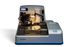
Dimension Icon
Bruker’s Dimension Icon brings the highest levels of performance, functionality, and AFM accessibility to nanoscale researchers in science and industry. Building upon the world’s most utilized large-sample AFM platform, it is the culmination of decades of technological innovation, customer feedback, and industry-leading application flexibility.

Dimension Icon AFM
The supplier does not provide quotations for this product through SelectScience. You can search for similar products in our Product Directory.
Bruker’s Dimension Icon® Atomic Force Microscope (AFM) System introduces new levels of performance, functionality, and AFM Dimension Icon is the most productive large-sample AFM in the world.
Bruker’s Dimension Icon Atomic Force Microscope (AFM) System introduces new levels of performance, functionality, and AFM accessibility to nanoscale researchers in science and industry. As the world’s most utilized large-sample AFM platform, the Dimension Icon is the culmination of decades of technological innovation, customer feedback, and industry-leading application flexibility. The system has been designed from top to bottom to deliver the revolutionary low drift and low noise that allows users to achieve artifact-free images
in minutes instead of hours. Icon also is fully optimized with proprietary PeakForce Tapping technology and ScanAsyst automatic image optimization technology, which enable easier, faster, and more consistent results, regardless of user skill level. Highest level AFM research with radical productivity gains has never been easier to achieve.
Dimension Icon is Bruker’s best-selling AFM for a host of reasons:
- Highest performance closed-loop tip scanning delivers unmatched large-sample resolution with open-loop noise levels, reduced noise floor, and <200 pm drift rates.
- Hardware and software optimized for productivity provides surprisingly simple setup, intuitive workflow, and fast time to results for publication-quality data every time.
- Open-access platform delivers unprecedented versatility to accommodate the widest variety of experiments, modes, techniques and semi-automated measurements.

Nanoscale mapping of permittivity and conductivity with scanning microwave impedance microscopy
Scanning microwave impedance microscopy (sMIM) is an atomic force microscopy (AFM)-based technique for materials and device characterization. The reflected microwave signal from the tip-sample interface holds information of the electrodynamic properties of the sample surface underneath the tip apex. In this application note from Bruker, explore sMIM and its integration with Bruker’s versatile AFM platforms, such as the Dimension Icon® and Dimension Edge™ AFMs. Furthermore, discover how when combined with Bruker’s exclusive PeakForce Tapping® mode, it is possible to obtain sMIM results on delicate samples, such as carbon nanotubes.
Improving the accuracy of nanomechanical measurements with force-curve-based AFM techniques
The structure and mechanical properties of sub-micron features in materials are of particular interest due to their influence on macroscopic material performance and function. Atomic force microscopy has the high resolution and force control to directly probe the mechanical properties of a wide range of these materials. In this application note from Bruker, consider the development and implementation of several new features that improve the flexibility, accuracy, and productivity of atomic force microscopes in measuring such important material properties as modulus and adhesion.
Performing hyperspectral mapping with AFM DataCube nanoelectrical modes
Atomic force microscopy (AFM)-based nanoelectrical modes have found applications in fields ranging from semiconductors to piezoelectric materials, energy research, and biology. Modes are available to characterize the local conductivity, resistivity, charge, carrier concentration, carrier-type, or piezoelectric properties with nanometer-scale spatial resolution, and usually require direct contact between the AFM tip and sample. In this application note, explore a new approach to nanoelectrical imaging that goes beyond a 2D map.
Measuring nanoscale viscoelastic properties with AFM-based nanoscale DMA
The development of heterogeneous materials like polymer composites, blends, and multilayers is of considerable importance in the chemicals industry. Bulk viscoelastic measurements are routine in establishing structure-property relationships for these materials. In this application note from Bruker, explore how the development of the AFM-nDMA™ mode, can avoid issues associated with measuring nanoscale viscoelastic properties and how the frequency and temperature dependence of viscoelastic properties in rheologically relevant ranges can be directly measured with 10 nm spatial resolution.
Deep learning to classify and establish structure property predictions with PeakForce QNM atomic force microscopy
Machine learning, is a powerful tool to establish the presence (or absence) of correlations between microstructure and bulk properties with its ability to flesh out relationships and trends that are difficult to establish otherwise. In this application note from Bruker, explore the use of deep learning tools, such as convolutional neural nets (CNNs), to explore atomic force microscopy (AFM) phase and PeakForce QNM® images of impact copolymers, a polymer blend of polypropylene with micro-sized domains of rubber.
Characterizing ferroelectric materials with SS-PFM and DCUBE PFM
Piezoresponse force microscopy (PFM) is a powerful technique for studying ferroelectric materials due to the high sensitivity and nanometer-level resolution that it inherits from atomic force microscopy (AFM). PFM-based spectroscopic methods, such as switching spectroscopy PFM (SS-PFM) and DataCube™ PFM (DCUBE PFM), allow the characterization of key parameters of ferroelectrics, such as coercive voltages, nucleation voltages, saturation responses, and more. Unfortunately, the quantification and interpretation of PFM results can be complicated by artifacts. In this application note from Bruker, learn more about the best modes and practices for optimizing PFM measurements to achieve reliable results.
Explore Bruker’s Dimension Icon atomic force microscope
In this application note, explore Bruker’s Dimension Icon® Atomic Force Microscope (AFM) System which offers new levels of performance, functionality, and AFM accessibility to nanoscale researchers in science and industry. This system has been designed from top to bottom to deliver the revolutionary low drift and low noise that allows users to achieve artifact-free images in minutes instead of hours. Icon is also fully optimized with proprietary PeakForce Tapping® technology and ScanAsyst® automatic image optimization technology, which enables easier, faster, and more consistent results, regardless of user skill level.
Explore the Dimension Edge with ScanAsyst
In this application note, explore the Dimension Edge™ Atomic Force Microscope (AFM) which incorporates Bruker’s PeakForce Tapping® technology to provide the high levels of performance, functionality, and accessibility. Based on the Dimension Icon® platform, the Edge system has been designed from top to bottom to deliver the low drift and low noise necessary to achieve publication-ready data in minutes instead of hours, all at price points well below expectations for such performance. Furthermore, explore how ScanAsyst® imaging, integrated visual feedback, and preconfigured settings enable expert-level results simply and consistently.
Quantitative mechanical property mapping at the nanoscale with PeakForce QNM
The scanning probe microscope (SPM) has long been recognized as a useful tool for measuring the mechanical properties of materials. Until recently though, it has been impossible to achieve truly quantitative material property mapping with the resolution and convenience demanded by SPM researchers. A number of recent SPM mode innovations have taken aim at these limitations, and now, with Bruker’s PeakForce QNM®, it is possible to identify material variations unambiguously and at high resolution across a topographic image. In this application note, explore the principles and benefits of the PeakForce QNM imaging mode.
Simultaneous electrical and mechanical property mapping at the nanoscale with PeakForce TUNA
Atomic force microscopy (AFM)-based conductivity measurements are a powerful technique for nanometer-scale electrical characterization on a wide range of samples. Tunneling AFM (TUNA), cover the lower current range (sub-pA up to nA). Bruker has developed an enhanced TUNA module with its proprietary PeakForce Tapping™ mode of operation that makes significant improvements to all three of these elements to enable exquisite tip-sample force control, quantitative nano-mechanical material property mapping through PeakForce QNM™, correlated nanoscale electrical property characterization through TUNA, and extreme ease of use through the ScanAsyst™ image optimization algorithms. A special probe has also been designed for use on particularly challenging samples. In this application note, explore the basics of PeakForce TUNA™, and compare it to standard Contact Mode–based TUNA.