Quantitative Mechanical Property Mapping at the Nanoscale with PeakForce QNM
4 Mar 2013The scanning probe microscope (SPM) has long been recognized as a useful tool for measuring mechanical properties of materials. Until recently though, it has been impossible to achieve truly quantitative material property mapping with the resolution and convenience demanded by SPM researchers. A number of recent SPM mode innovations have taken aim at these limitations, and now, with Bruker’s PeakForce QNM®, it is possible to identify material variations unambiguously and at high resolution across a topographic image. This application note discusses the principles and benefits of the PeakForce QNM imaging mode.
Related products
Request Quote for All Products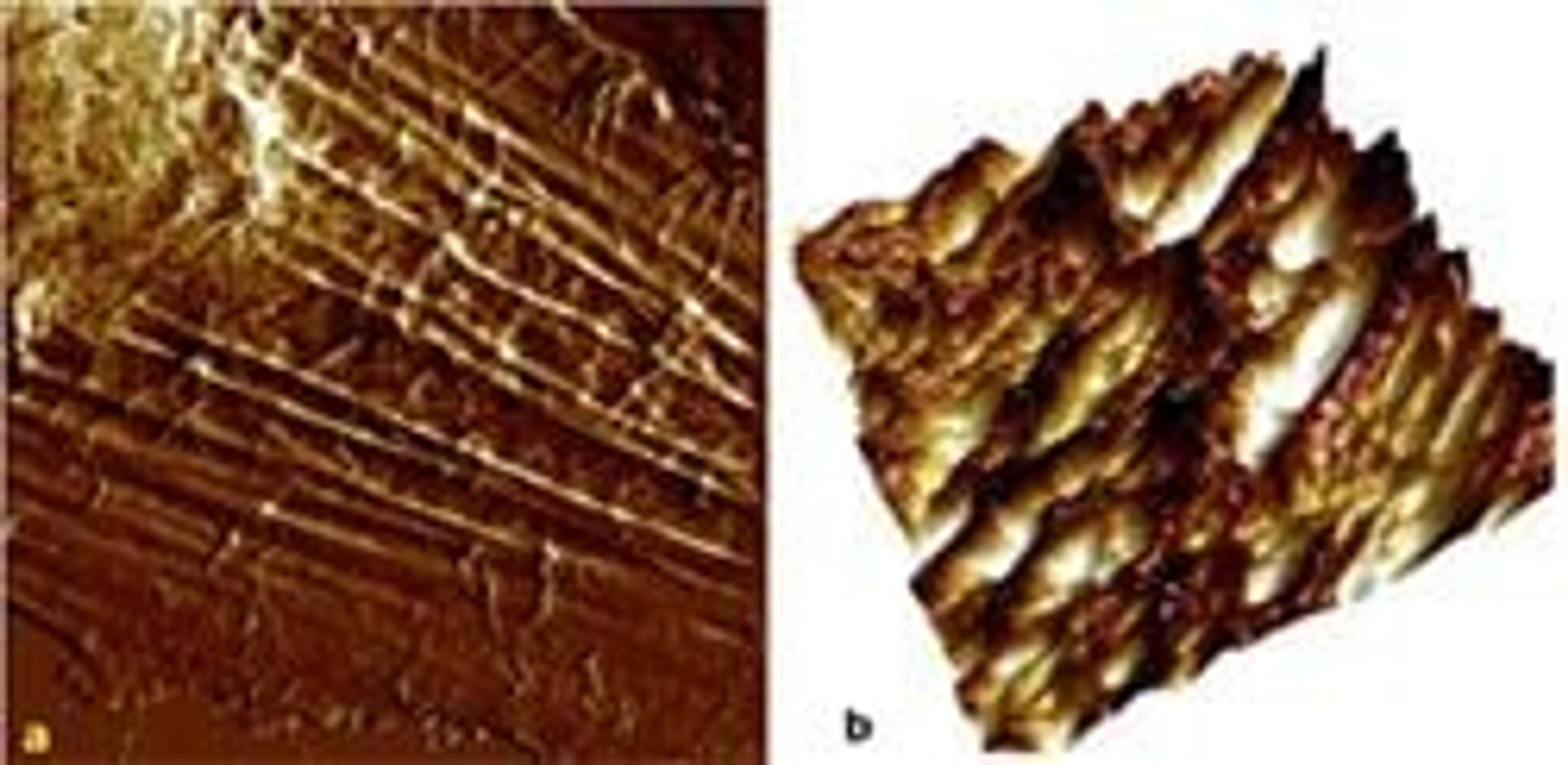
PeakForce QNM
Bruker Nano Surfaces and MetrologyUnprecedented quantitative characterization of materials on the nanoscale PeakForce QNM® (Quantitative Nanomechanical Property Mapping) allows quantitative nanomechanical mapping of material properties, including modulus and adhesion, while simultaneously imaging sample topography at high resolution. PeakForce QNM and its counterpart mode PeakForce Mapping are based on Bruker's exclusive PeakForce Tapping® technology, which records very fast force response curves at every pixel in the image. The force control made possible by this technique leads to longer probe lifetimes and improved sample integrity, as well as correlated, high-resolution nanomechanical and topographic data. These capabilities dramatically exceed those of any other technique for nanoscale materials characterization, changing the perception and use of AFM.