ResourceMaterials
ArBlade 5000 – An innovative, high-performance sample preparation tool for SEM
7 Apr 2025Often, conventional mechanical sample preparation techniques for scanning electron microscopy (SEM) can deliver usable results on some specimens. However, they can also fail, especially when it comes to composites and layered structures with different hardness, brittle materials, and so forth. Explore the power of broad ion beam milling methods and how the Hitachi ArBlade 5000 – a broad ion beam system – produces exceptionally high-quality cross-section or flat-milling samples for electron microscopy.
Related products
Request Quote for All Products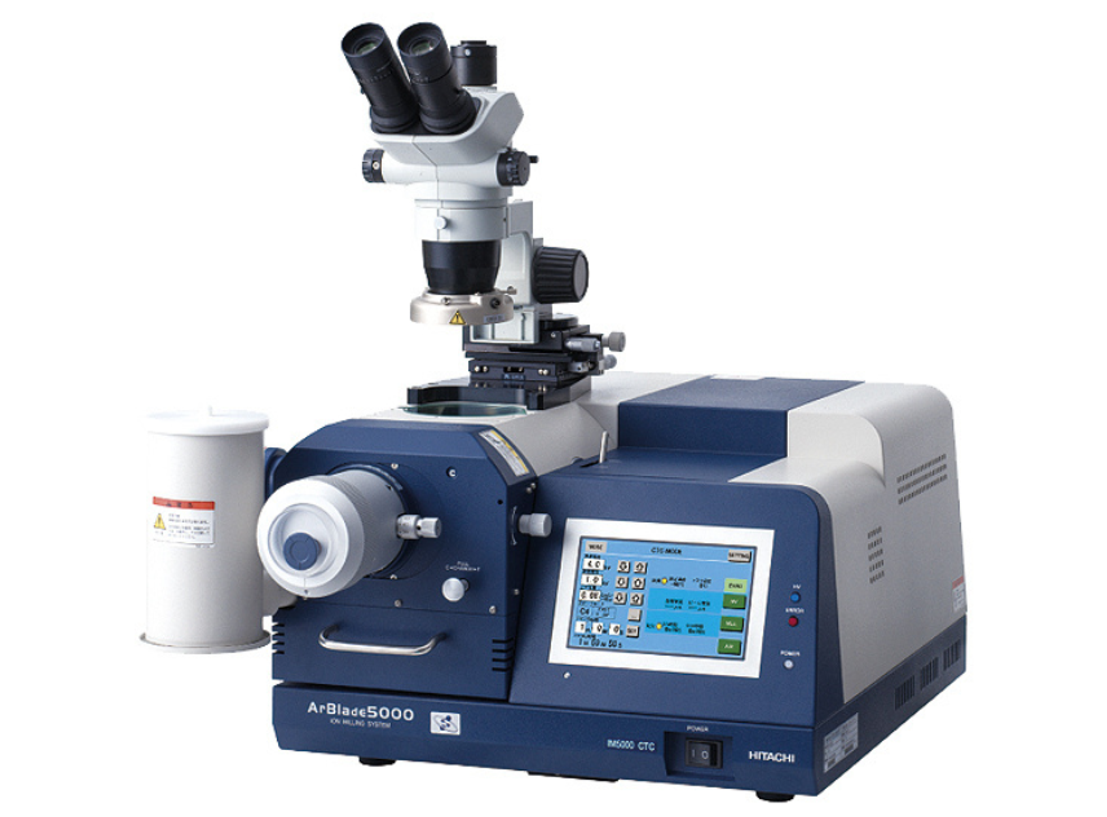
Links
Tags
Electron MicroscopyElectron microscopes (EM) are used to create high-resolution images of samples at the nanoscale by means of an accelerated beam of electrons as a source of illumination. Types of electron microscope include scanning electron microscopes (SEM), transmission electron microscopes (TEM), scanning transmission electron microscopes (STEM) and cryo-electron microscopes. Focused ion beam (FIB) microscopes are useful for modifying or milling a sample surface with nanometer precision, as well as imaging. Find the best electron microscopes in our peer-reviewed product directory: compare products, check customer reviews and receive pricing direct from manufacturers.Mills, Sieves and PressesMills, sieves and presses are used to break and sort solid materials into smaller particle sizes for further processing such as pellet pressing or analysis. Milling equipment includes grinders, ball mills, cutting mills, jaw crushers, knife mills, beater and planetary mills. Sorting of smaller particulates can be achieved with test sieves and sieve shakers. Final powders can be pressed with hydraulic presses. Milling and pressing solid samples is an important preparation step in X-ray fluorescence spectroscopy (XRF) and diffraction (XRD). Find the best mills, sieves and presses in our peer-reviewed product directory: compare products, check customer reviews and receive pricing direct from manufacturers.SEMScanning Electron Microscopy (SEM) is a technique that uses a focused electron beam to scan a sample and create high-resolution images. It is widely used in materials science, nanotechnology, and biological research. Explore SEM systems in our peer-reviewed product directory; compare products, check reviews, and get pricing directly from manufacturers.Argon