ResourceSpectroscopy
Nanometer Scale EDS Analysis using Low-kVFE-SEM and Windowless EDS Detector
15 May 2017Characterizing structures on a nano-scale is challenging as the resolution of EDS analysis is usually limited to micrometers. This application note describes a method which combines scanning electron microscopy (SEM) with energy dispersive X-ray spectroscopy (EDS). The study used a combination of the X-Max Extreme – a high resolution, low kV SEM and a windowless EDS detector – and the ZEISS GeminiSEM 500 and was able to achieve a resolution of 10nm and less, allowing investigation of the morphology and chemistry of nano-structures.
Related products
Request Quote for All Products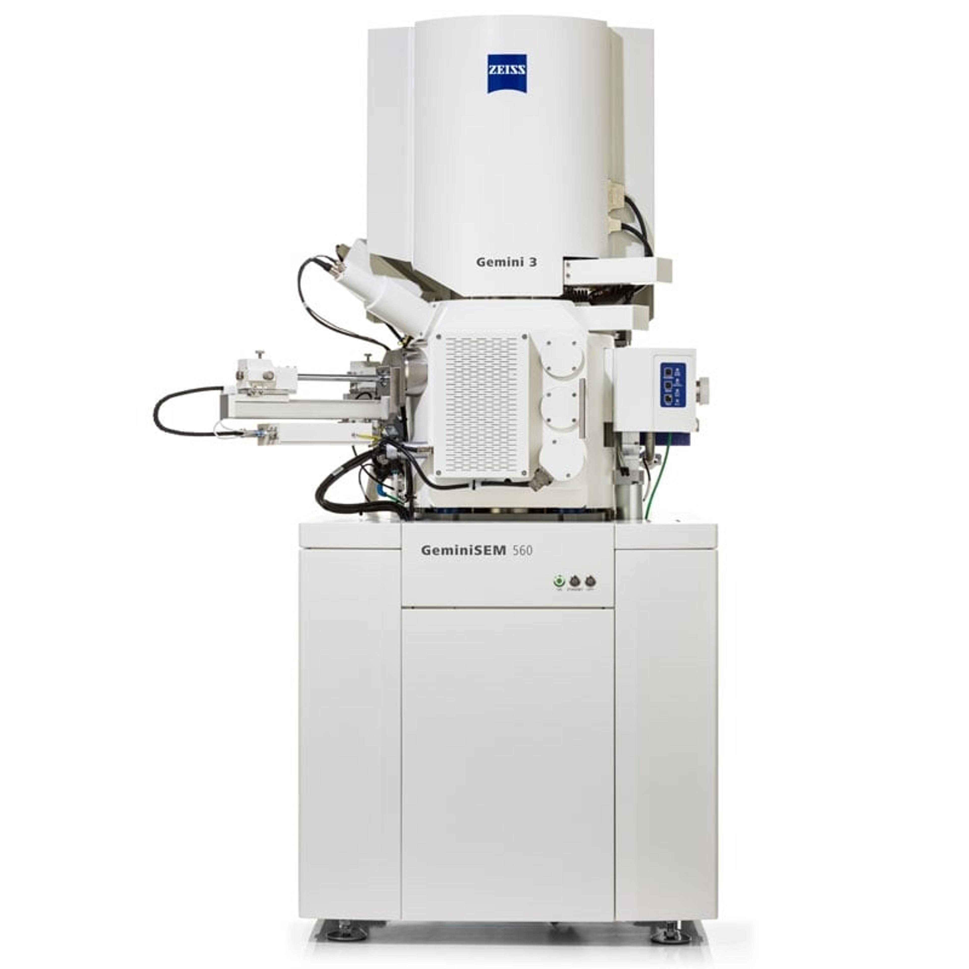
ZEISS GeminiSEM Family
ZEISS Research Microscopy SolutionsFor Your Highest Demands in Sub-nanometer Imaging, Analytics and Sample Flexibility
Links
Tags
X-Ray Diffraction and SpectroscopyX-Ray diffraction & spectroscopy are used in material characterization to discern the structure and elemental composition of a sample. X-Ray diffractometers (XRD) are superior instruments in elucidating the dimensional atomic structure of crystalline materials, including powders, thin films and single crystals. For large unit cells or ordered macromolecules, consider small-angle X-ray scattering (SAXS). X-ray spectroscopic techniques include X-ray fluorescence (XRF) and X-ray photoelectron spectroscopy (XPS), both providing simple and accurate methods for determining the elemental composition of a material. Energy dispersive (EDXRF) and wavelength dispersive (WDXRF) XRF spectrometers are available, as well as handheld/portable devices. High-resolution, 3D microstructure characterization of materials can be achieved with X-ray microscopes combining sub-micron resolution imaging with 3D computed tomography. Find the best XRD and XRF spectrometers in our peer-reviewed product directory: compare products, check customer reviews and receive pricing direct from manufacturers.Electron MicroscopyElectron microscopes (EM) are used to create high-resolution images of samples at the nanoscale by means of an accelerated beam of electrons as a source of illumination. Types of electron microscope include scanning electron microscopes (SEM), transmission electron microscopes (TEM), scanning transmission electron microscopes (STEM) and cryo-electron microscopes. Focused ion beam (FIB) microscopes are useful for modifying or milling a sample surface with nanometer precision, as well as imaging. Find the best electron microscopes in our peer-reviewed product directory: compare products, check customer reviews and receive pricing direct from manufacturers.NanotechnologyNanotechnology, or nanotech, is an engineering technique using molecular scale functional systems. Applications of nanotechnology include medicine and medical devices, electronics, air and water purification, food science and energy production.NanostructuresSEMScanning Electron Microscopy (SEM) is a technique that uses a focused electron beam to scan a sample and create high-resolution images. It is widely used in materials science, nanotechnology, and biological research. Explore SEM systems in our peer-reviewed product directory; compare products, check reviews, and get pricing directly from manufacturers.NanoparticlesNanoparticles are between 1-100nm in size. Nanoparticles can be used for a wide variety of applications including biomedical, catalysis and electronics.