ResourceMaterials
Making the connection: Atomic force microscopy correlates Graphene's functional properties on the nanoscale
19 May 2021Download this application note to discover how a combination of different AFM techniques allows a holistic and in-depth characterization of 2D materials as demonstrated on a wafer-scale CVD-grown graphene on sapphire produced in an Aixtron CCS R&D reactor.
Related products
Request Quote for All Products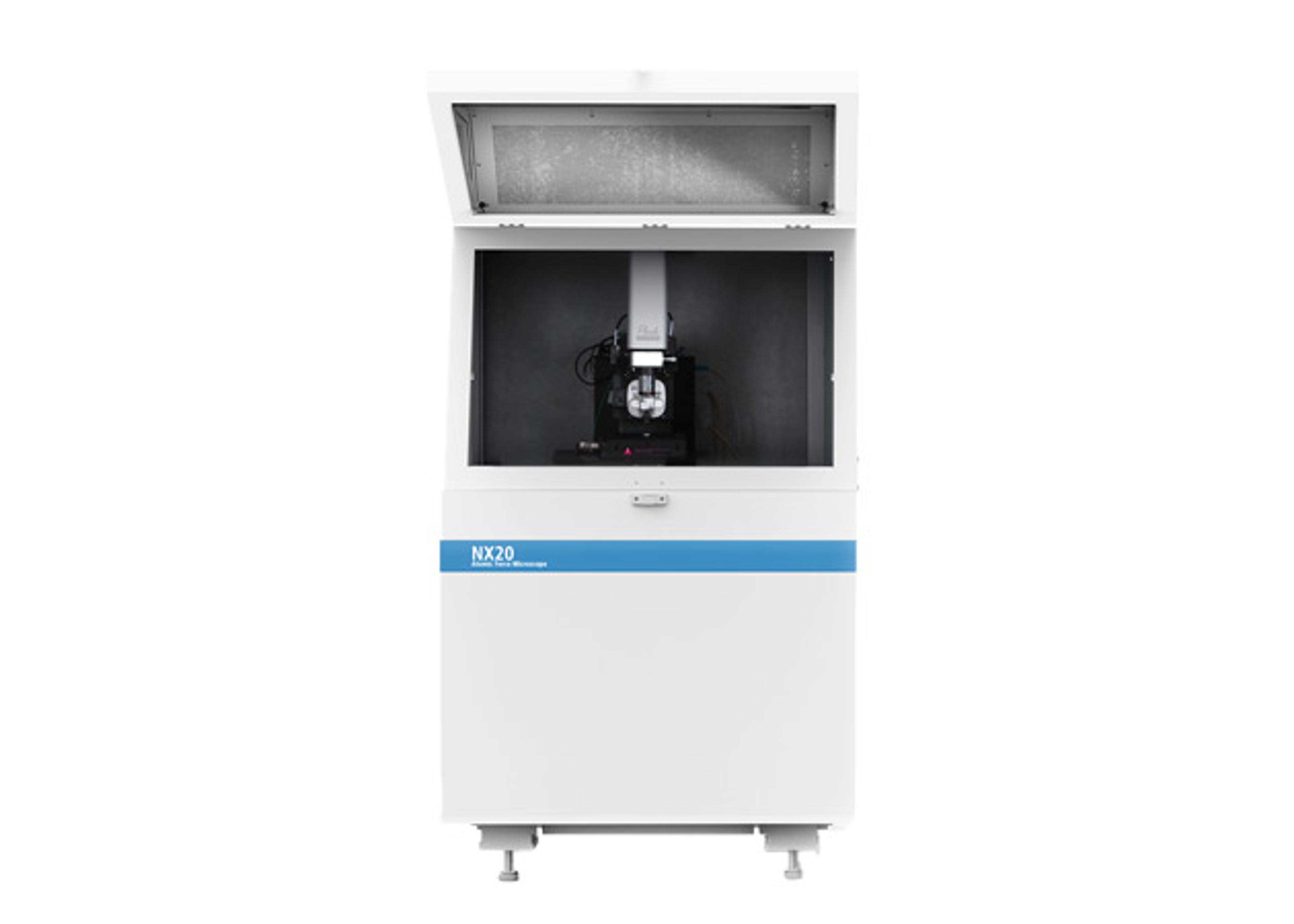
Park NX20 Atomic Force Microscope
Park SystemsAdvanced research AFM for high-resolution surface and materials analysis
Links
Tags
NanotechnologyNanotechnology, or nanotech, is an engineering technique using molecular scale functional systems. Applications of nanotechnology include medicine and medical devices, electronics, air and water purification, food science and energy production.Atomic Force Microscopy / Scanning Tunneling MicroscopyAtomic force microscopes (AFM) and scanning tunneling microscopes (STM) are high-resolution forms of scanning probe microscope (SPM) used to generate topological information of a sample down to the atomic scale. Instruments can generate an image of the surface topology, manipulate objects and reveal information on localized properties such as Young’s modulus, conductivity, and magnetism. High-quality STM and AFM probes optimized for your application are available, as well as other SPM-based instruments such as scanning ion conductance microscopes (SICM) & near-field scanning optical microscopes (NSOM). Find the best AFM and STM equipment in our peer-reviewed product directory: compare products, check customer reviews and receive pricing direct from manufacturers.AFMGrapheneGraphene is a two-dimensional structure that comprises of a hexagonal honeycomb lattice of carbon atoms. Graphene can conduct electricity and heat, is almost transparent and is 100x stronger than steel by weight.NanostructuresNanomaterialsNanomaterials such as carbon nanotubes, fullerenes and nanoparticles are a group of materials that measure between 1-1000nm for a single unit. Analysis techniques include AFM, electron microscopy and super resolution microscopy.2D Materials