Hysitron PI Series PicoIndenters
24 Jul 2023In this application note, Bruker Nano provides an overview of its Hysitron® PI Series PicoIndenters® for quantitative nanomechanics. These nanomechanical testing systems allow you to conduct in-situ mechanical experiments in your scanning electron microscope (SEM) or transmission electron microscope (TEM). The unique transducer design promises to deliver stability throughout your experiments, resulting in precise data even at the nanoscale. Video capture from the microscope enables real-time monitoring and direct correlation of mechanical data to microscope imaging.
Related products
Request Quote for All Products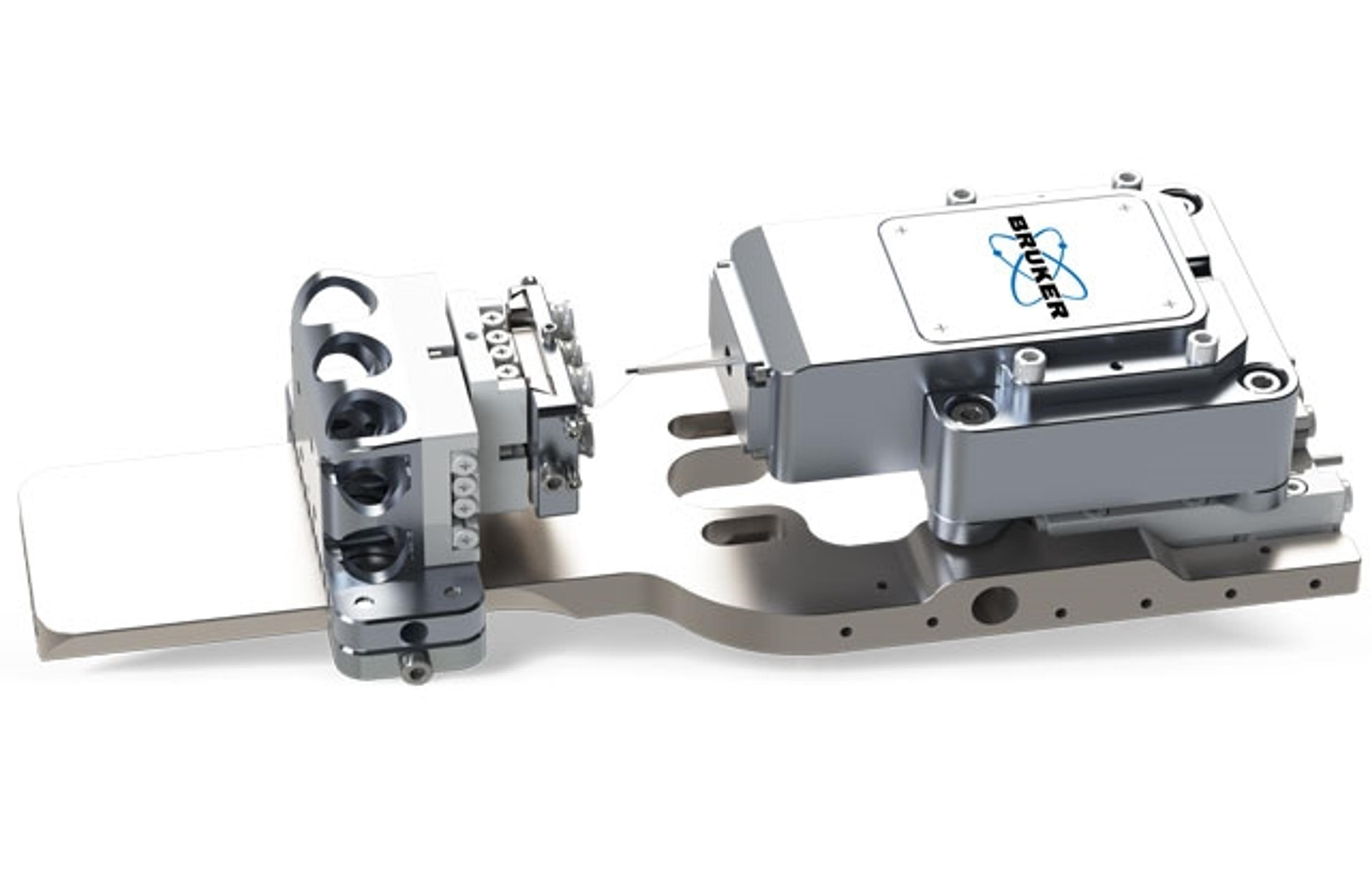
Hysitron PI 89
Bruker Nano Surfaces and MetrologyThe Hysitron PI 89 SEM PicoIndenter leverages the advanced imaging capabilities of scanning electron microscopes (SEM, FIBSEM, PFIB), making it possible to perform quantitative nanomechanical testing while simultaneously imaging. Enabled testing techniques include nanoindentation, tensile testing, pillar compression, particle compression, cantilever bending, fracture, fatigue, dynamic testing, and mechanical properties mapping.