High Resolution STEM and EDS FIB-SEM Study of Chromium Depletion in Stainless Steel
High Resolution STEM and EDS FIB-SEM Study of Chromium Depletion in Stainless Steel
16 Mar 2016This application note describes a study of heat affected X2CrNi18-10 stainless steel. Small chromium carbide particles form at the grain boundaries of the material, causing chromium depletion of the surrounding matrix and thus promoting corrosion. A thin lamella was prepared at a grain boundary and analyzed with scanning transmission electron microscopy (STEM) and energy dispersive spectroscopy (EDS) by a ZEISS FIB-SEM instrument. The EDS results obtained on the lamella show a spatial resolution of the order of 10 nm and allow the extent of the chromium depletion to be qualitatively determined.
Related products
Request Quote for All Products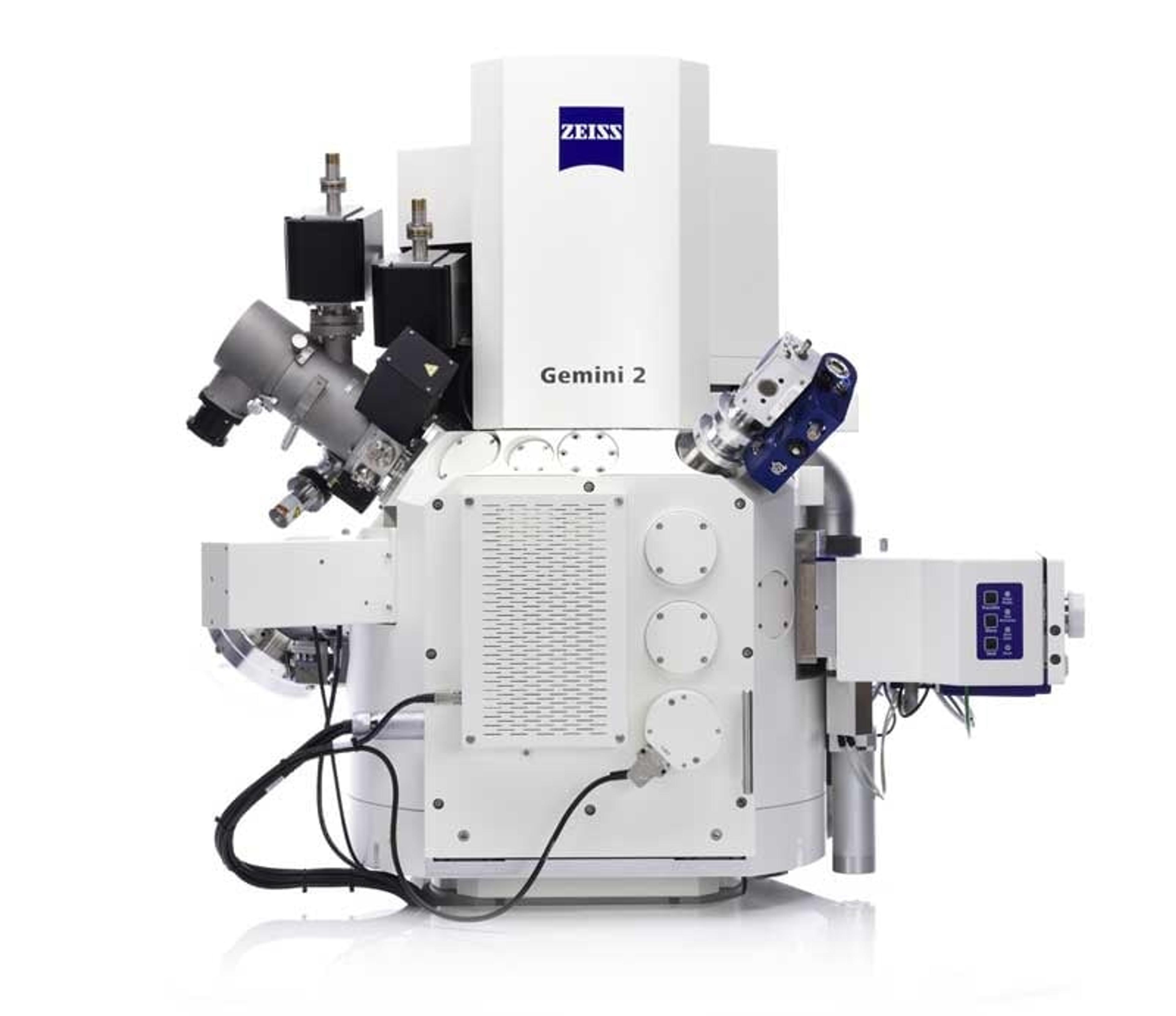
ZEISS Crossbeam Family
ZEISS Research Microscopy SolutionsWithin ZEISS Crossbeam Family you have the choice between Crossbeam 340 or Crossbeam 550. Exploit the variable pressure capabilities of Crossbeam 340. Or use Crossbeam 550 for your most demanding characterizations and choose the chamber size, standard or large, that best suits your samples.