Evolution of Gemini electron optics: The next chapter in sub-nanometer imaging below 1 kV
25 Feb 2021In the last 20 years, a major thrust of research in scanning electron microscopy (SEM) has been driving the performance of systems towards higher resolution at lower voltages. Key to the performance of any SEM, conventional or field emission SEM (FE-SEM), is its electron optical column.
In this application note, ZEISS demonstrate the evolution of their FE-SEMs, which are based upon the Gemini column design which has seen a number of technological advancements since it was first launched in 1993. The latest development in this field is the new engine Smart Autopilot which provides further increases in resolution at low kV by optimizing the convergence angle of
electrons travelling through the column at given conditions.
Related products
Request Quote for All Products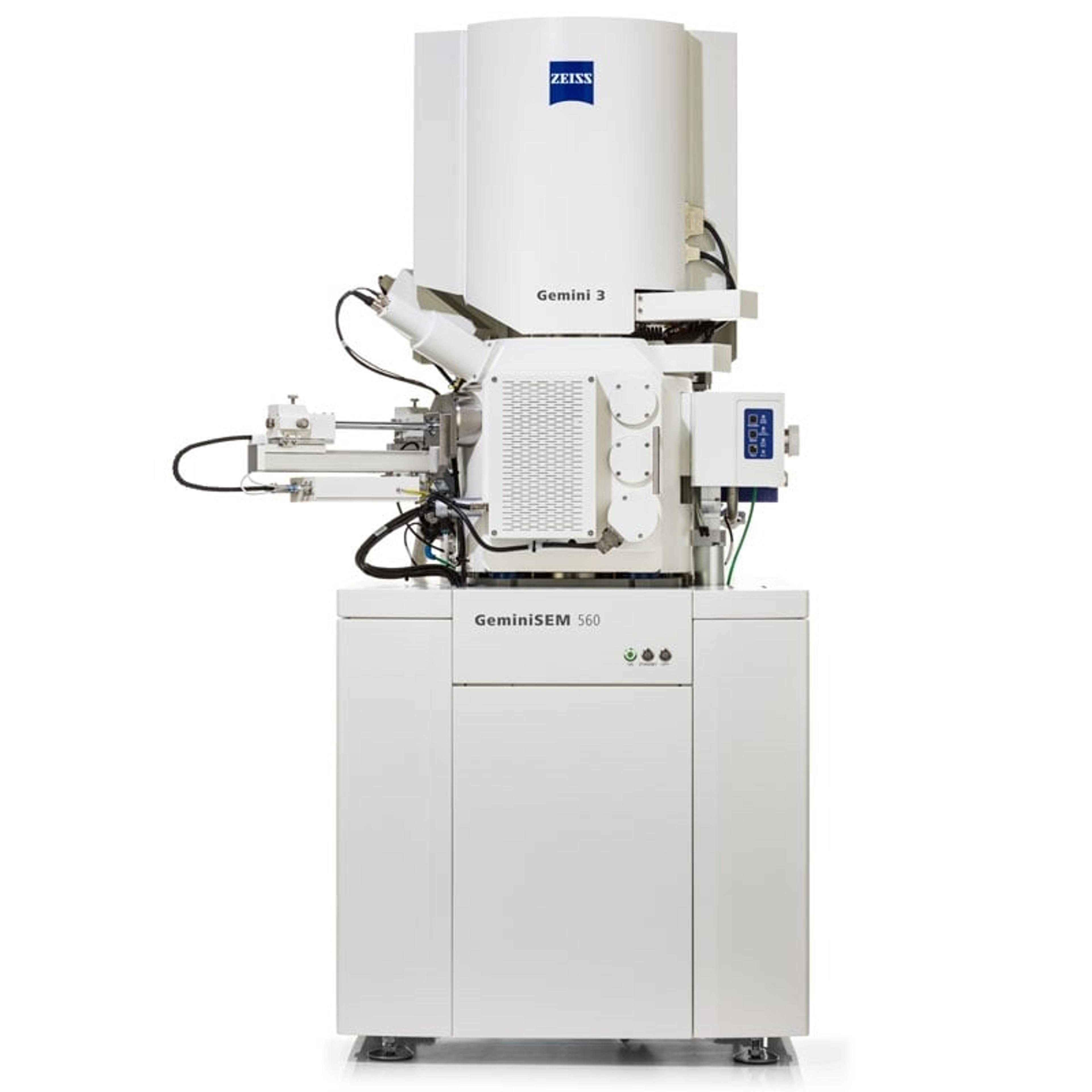
ZEISS GeminiSEM Family
ZEISS Research Microscopy SolutionsFor Your Highest Demands in Sub-nanometer Imaging, Analytics and Sample Flexibility