ResourceMaterials
Electron Channeling Contrast Imaging Performed by ZEISS GeminiSEM 500
18 Sept 2017Electron channeling contrast imaging (ECCI) is a technique for quantitative characterization of deformation structures in scanning electron microscopy (SEM). Relative orientation of crystalline lattice and incident electron beam influence back scattered electrons. ECCI makes use of this. ECCI in SEM is especially useful for imaging crystallographic defects such as dislocations, stacking faults and twin boundaries and thus starts to have an impact on materials science. This application note describes the electron channeling contrast imaging of crystalline defects using ZEISS GeminiSEM 500.
Related products
Request Quote for All Products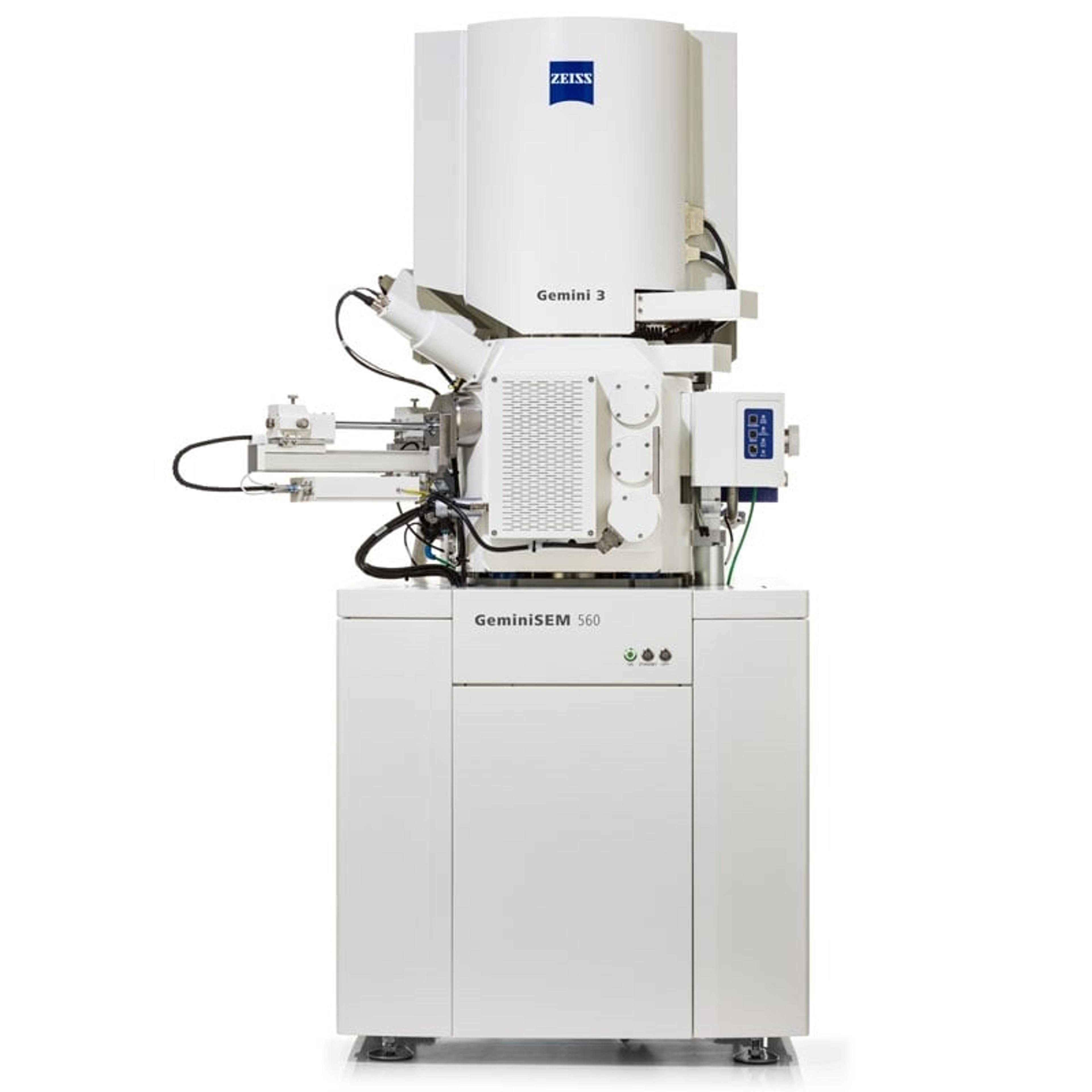
ZEISS GeminiSEM Family
ZEISS Research Microscopy SolutionsFor Your Highest Demands in Sub-nanometer Imaging, Analytics and Sample Flexibility
Links
Tags
Electron MicroscopyElectron microscopes (EM) are used to create high-resolution images of samples at the nanoscale by means of an accelerated beam of electrons as a source of illumination. Types of electron microscope include scanning electron microscopes (SEM), transmission electron microscopes (TEM), scanning transmission electron microscopes (STEM) and cryo-electron microscopes. Focused ion beam (FIB) microscopes are useful for modifying or milling a sample surface with nanometer precision, as well as imaging. Find the best electron microscopes in our peer-reviewed product directory: compare products, check customer reviews and receive pricing direct from manufacturers.ImagingImaging techniques are essential for obtaining visual representations of samples to understand structures, processes, and function in biological, chemical, and physical research. These tools range from traditional light microscopy to advanced imaging modalities like MRI and electron microscopy, providing researchers with valuable data for diagnostics, drug discovery, and material analysis. Explore imaging solutions in our peer-reviewed product directory to compare products, check reviews, and get pricing directly from manufacturers.MicroscopyMicroscopy is a technique used to observe small objects in detail, from cells to materials, using light or electron microscopes. It enables researchers to examine structures with high resolution, aiding in fields such as biology, medicine, and materials science. With advanced microscopy techniques, scientists can gain insights into cellular processes, tissue structures, and material properties. Explore the best microscopy solutions in our peer-reviewed product directory, compare products, read customer reviews, and get pricing directly from manufacturers.SEMScanning Electron Microscopy (SEM) is a technique that uses a focused electron beam to scan a sample and create high-resolution images. It is widely used in materials science, nanotechnology, and biological research. Explore SEM systems in our peer-reviewed product directory; compare products, check reviews, and get pricing directly from manufacturers.Crystallography