Direct pull tension testing with the Hysitron PI 89 SEM PicoIndenter - A primer
23 Jul 2023The tensile test is the most ubiquitous method for macroscale mechanical characterization of materials. This is because it provides a full stress strain curve, allowing analysis of such important material properties as yield strength, ultimate strength, elastic limit, and work hardening rates. In-situ nanomechanical testing is a powerful family of techniques that allow for real-time observation of deformation mechanisms that are directly correlated to load-displacement data.
The combination of these techniques with high-resolution electron microscopy and its related chemical and structural analysis techniques can provide incredibly detailed data. In this application note, Bruker Nano discusses using the Hysitron® PI 89 SEM PicoIndenter® and Tribo iQ™ application for direct pull tension within an SEM application, including the steps required for tip and sample fabrication, tip alignment, and data analysis.
Related products
Request Quote for All Products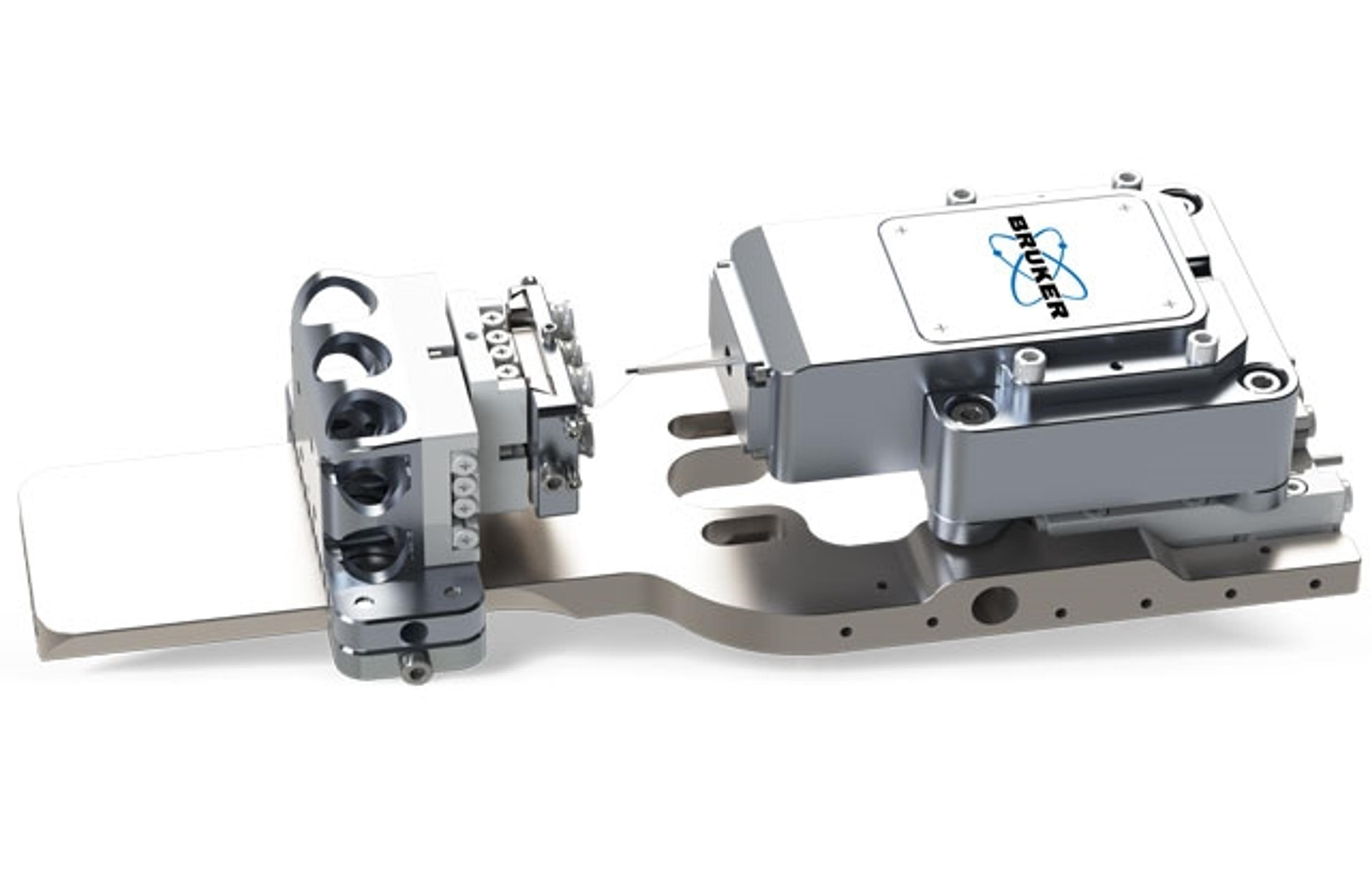
Hysitron PI 89
Bruker Nano Surfaces and MetrologyThe Hysitron PI 89 SEM PicoIndenter leverages the advanced imaging capabilities of scanning electron microscopes (SEM, FIBSEM, PFIB), making it possible to perform quantitative nanomechanical testing while simultaneously imaging. Enabled testing techniques include nanoindentation, tensile testing, pillar compression, particle compression, cantilever bending, fracture, fatigue, dynamic testing, and mechanical properties mapping.