DektakXT Stylus Profiler
25 Jun 2023In this application note, Bruker Nano provides a detailed overview of the DektakXT® Stylus Profiler. Offering high-quality performance, ease of use, and value, the DektakXT is designed to facilitate better process monitoring from R&D to QC. Dektak® innovation enables critical nanometer-level surface measurements for the microelectronics, semiconductors, solar, high-brightness LED, medical, and materials science industries.
Related products
Request Quote for All Products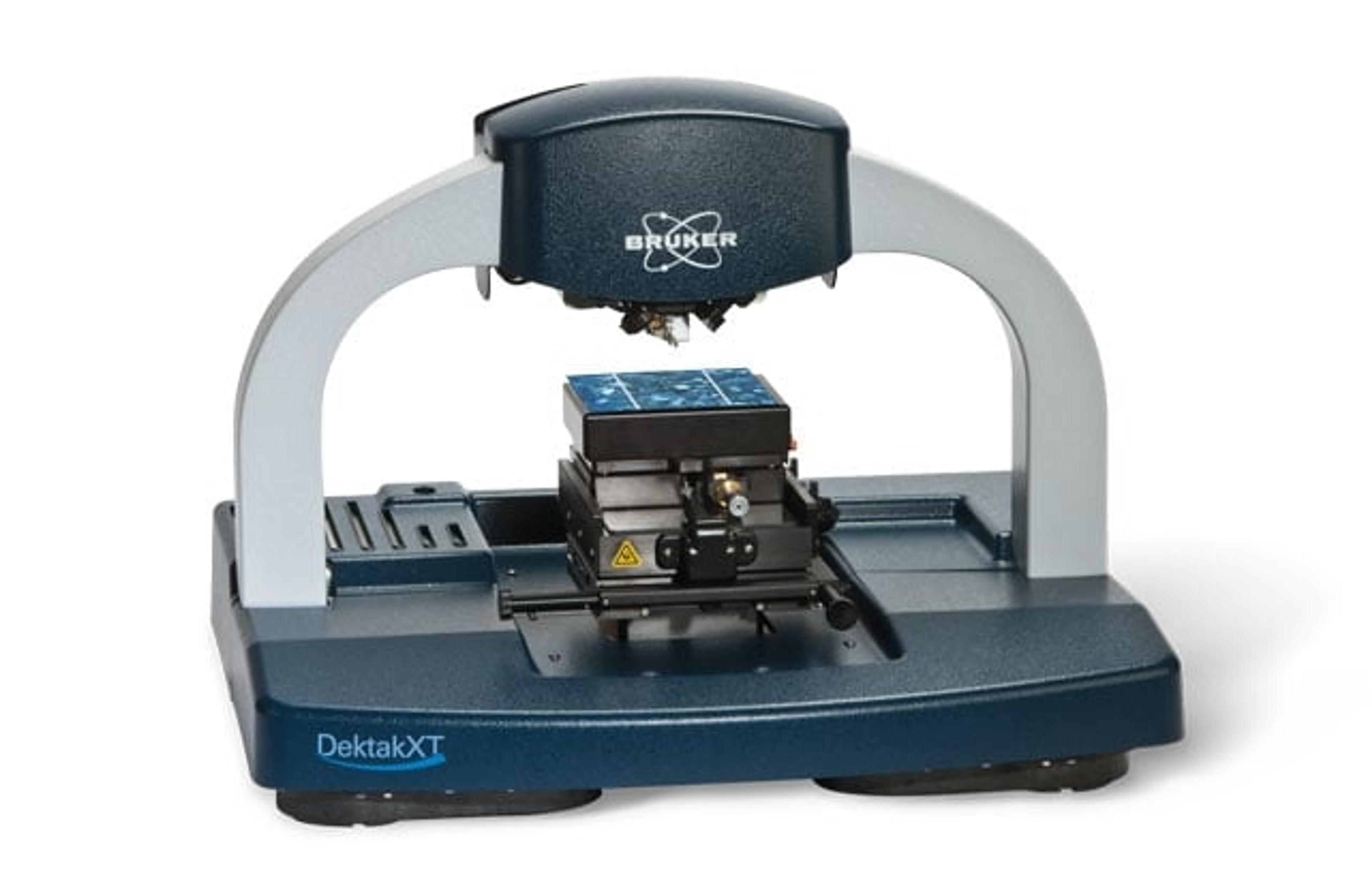
DektakXT
Bruker Nano Surfaces and MetrologyThe DektakXT stylus profilometer features a revolutionary benchtop design that enables an unmatched repeatability of 4 Å and up to 40% improvement in scanning speeds. The technological breakthroughs incorporated in DektakXT enable critical nanometer-level surface measurements for the microelectronics, semiconductor, solar, high-brightness LED, medical, and materials science industries.