ResourceLife Sciences
Combining AFM and SEM for High Performance Visualization
19 Jul 2018ZEISS in situ AFM optics integrates the best qualities of AFM and SEM to deliver high-performance in visualizing 3D topography down to the atomic level while measuring a wide range of physical properties. To find out more about the applications of in situ AFM, check out the appnote below.
Related products
Request Quote for All Products
ZEISS GeminiSEM for Life Sciences
ZEISS Research Microscopy SolutionsFor the Highest Demands in Imaging and Analytics from Any Sample
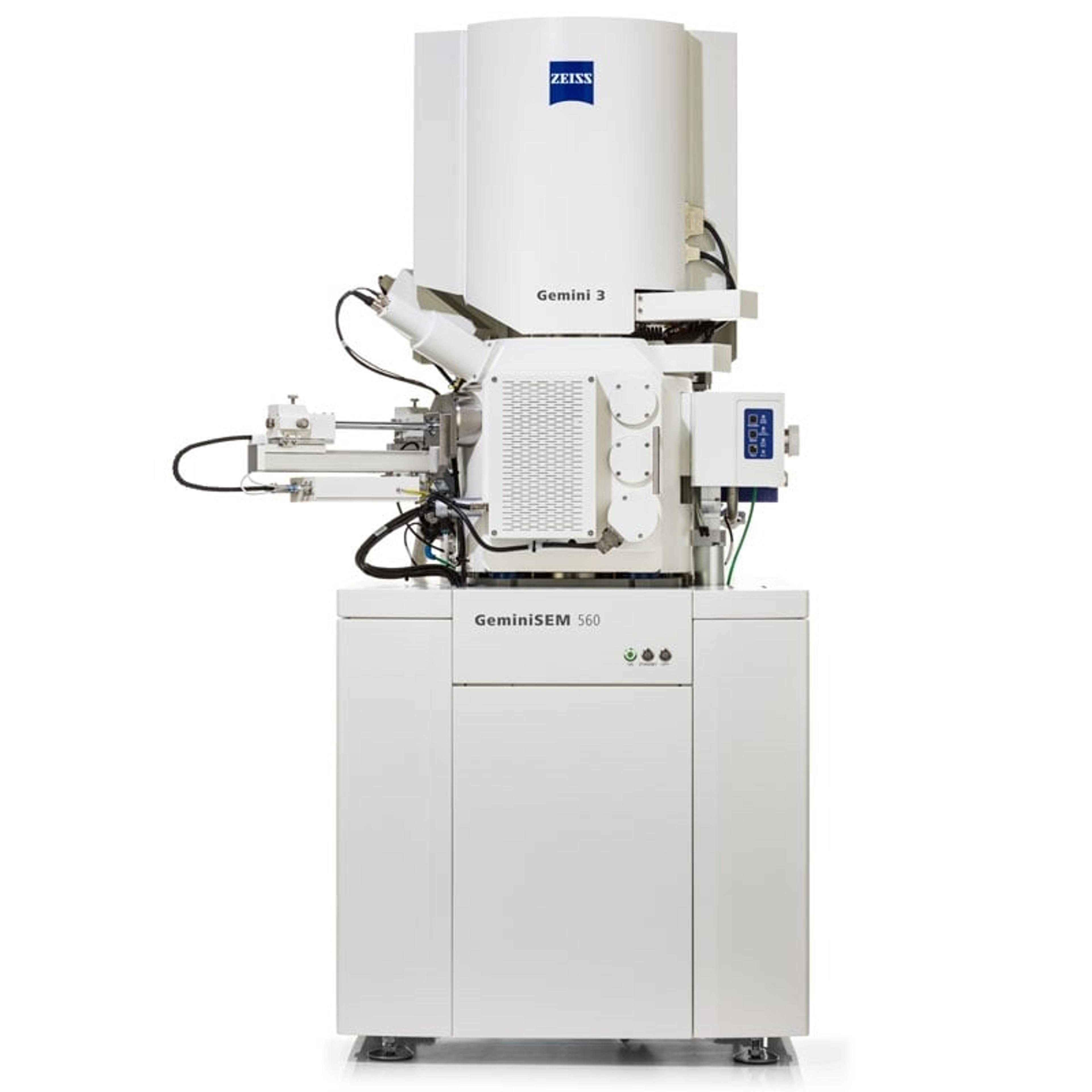
ZEISS GeminiSEM Family
ZEISS Research Microscopy SolutionsFor Your Highest Demands in Sub-nanometer Imaging, Analytics and Sample Flexibility
Links
Tags
Electron MicroscopyElectron microscopes (EM) are used to create high-resolution images of samples at the nanoscale by means of an accelerated beam of electrons as a source of illumination. Types of electron microscope include scanning electron microscopes (SEM), transmission electron microscopes (TEM), scanning transmission electron microscopes (STEM) and cryo-electron microscopes. Focused ion beam (FIB) microscopes are useful for modifying or milling a sample surface with nanometer precision, as well as imaging. Find the best electron microscopes in our peer-reviewed product directory: compare products, check customer reviews and receive pricing direct from manufacturers.Molecular BiologyMolecular biology is the branch of biology that focuses on the molecular mechanisms that underlie cellular functions. It involves studying DNA, RNA, and proteins to understand gene expression, replication, and regulation. Molecular biology is fundamental to biotechnology, medicine, and genetic research. Explore molecular biology products in our peer-reviewed product directory; compare products, check reviews, and get pricing directly from manufacturers.3D Imaging3D imaging technologies allow for the visualization and analysis of three-dimensional structures at high resolution. These systems are used in fields like molecular biology, material science, and medical diagnostics. 3D imaging can be applied to visualize cells, tissues, and organs, providing valuable insights into their structure and function. Browse our peer-reviewed product directory to find the best 3D imaging solutions, compare products, check reviews, and get pricing directly from manufacturers.Structural BiologyAFMNanostructuresSEMScanning Electron Microscopy (SEM) is a technique that uses a focused electron beam to scan a sample and create high-resolution images. It is widely used in materials science, nanotechnology, and biological research. Explore SEM systems in our peer-reviewed product directory; compare products, check reviews, and get pricing directly from manufacturers.