ResourceMaterials
Characterization of Amorphous and Microcrystalline Silicon Using Raman Spectroscopy
3 Feb 2015Silicon deposited on glass or silicon carbide is widely used in manufacturing photovoltaic cells. Raman spectroscopy is an ideal technique for this application. By mapping an area of deposited silicon the uniformity of the distribution of the two silicon forms can be monitored. This application note shows typical results and discusses some of the practical aspects and potential pitfalls of using Raman spectroscopy for measuring amorphous and crystalline silicon.
Related products
Request Quote for All Products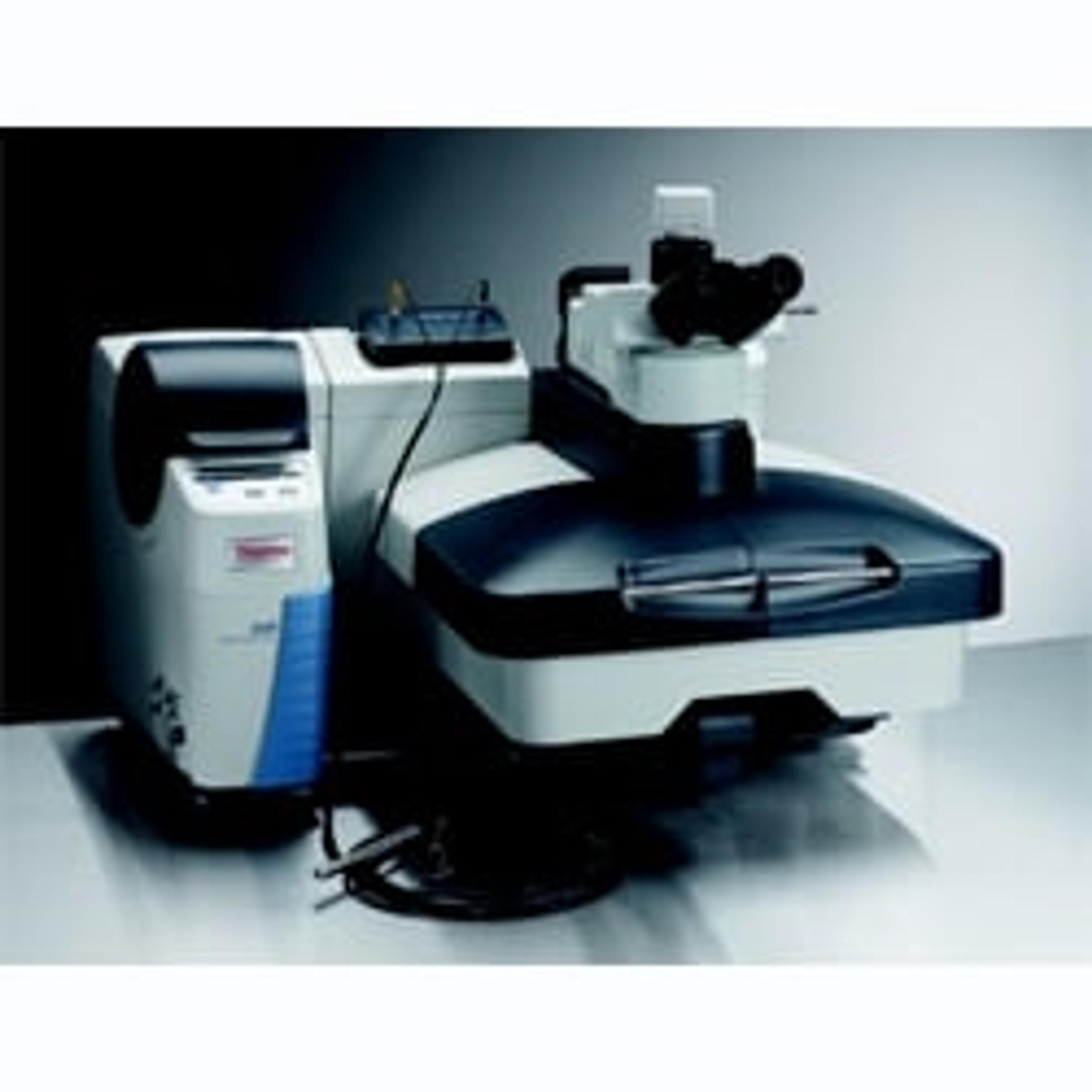
Thermo Scientific™ DXR3 Raman Microscope
Thermo Fisher ScientificAchieve exceptional sensitivity and spatial resolution for working applications with the Thermo Scientific DXR3 Raman microscope.
Links
Tags
Raman SpectroscopyRaman spectroscopy is used to discern the vibrational and rotational states of molecules and hence the chemical composition of a sample by measuring the inelastic scattering of monochromatic light. Explore a range of Raman spectrometers, including handheld/portable Raman spectrometers for QC/QA labs and in situ spectrometers for processes. Conduct Raman imaging for microanalysis of mixed samples using a Raman microscope. Raman spectrographs are also available. Find the best Raman spectroscopy products in our peer-reviewed product directory: compare products, check customer reviews and receive pricing direct from manufacturers.Solar EnergyPhotovoltaic Materials