ResourceMaterials
Axia ChemiSEM: Instant fusion of chemistry and imaging
19 Feb 2021In this datasheet, Thermo Fisher Scientific outlines the key benefits, technical highlights, and system specifications of the Axia ChemiSEM, a new generation of SEM. Download the full article to learn more about how this system is designed to provide an always-ready-to-image platform with unique live quantitative EDS mapping and can be used for the rapid analysis of a wide variety of different material types.
Related products
Request Quote for All Products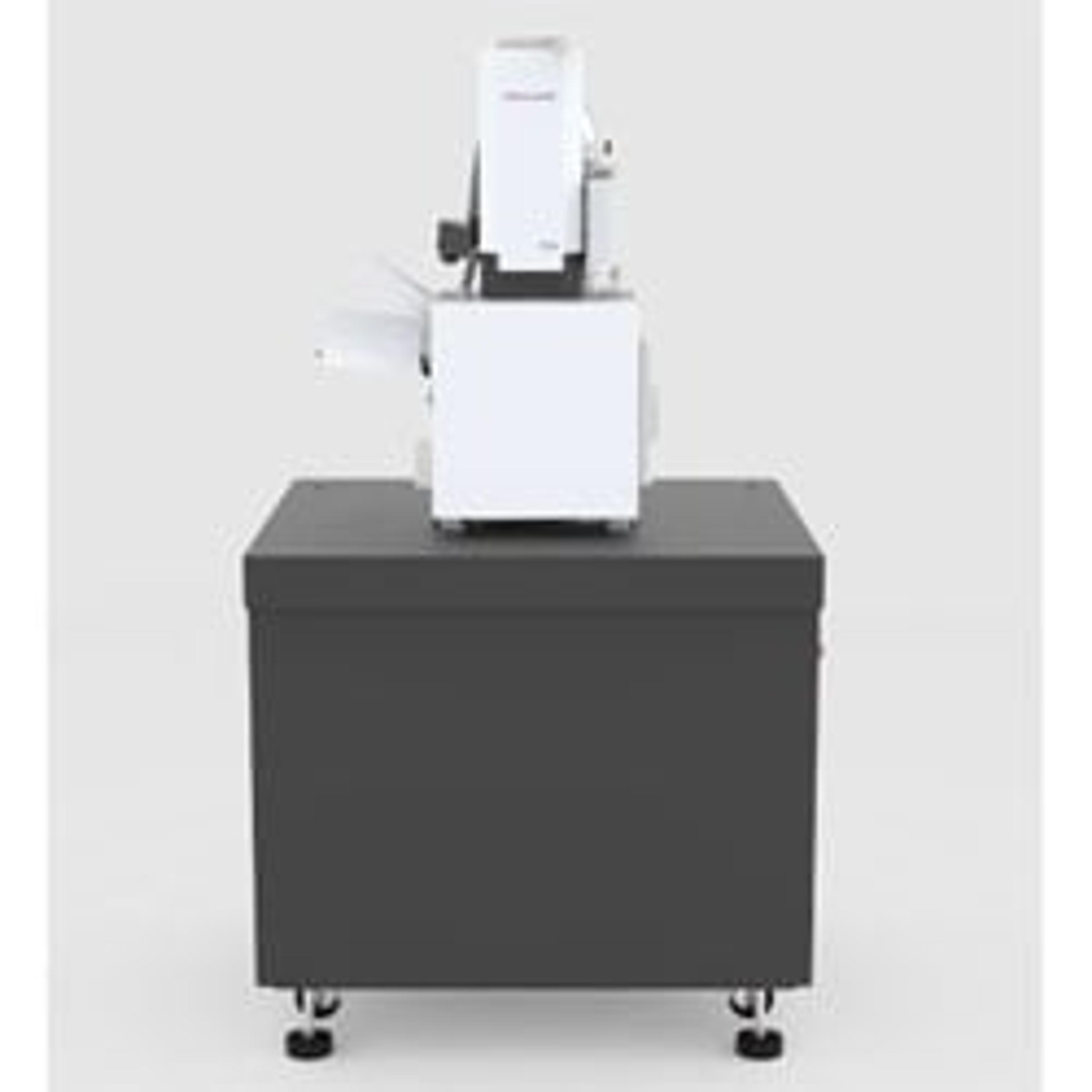
Thermo Scientific™ Axia ChemiSEM™ Scanning Electron Microscope
Thermo Fisher ScientificSEM EDS instrument that is flexible, easy to use, and offers instantaneous, quantitative elemental analysis.
Links
Tags
Particle CharacterizationParticle characterization instruments are used to determine particle size distribution, shape, surface area, zeta potential, density and porosity of particles and materials. Multiple tecchniques are available for determining particle size, shape and count including dynamic light scattering (DLS), laser diffraction, electrozone (Coulter technique), imaging particle analysis and single particle optical sensing. Determine the density of your material with a gas pycnometer or examine its surface area and porosity with gas adsorption analyzers and mercury porosimeters. Find the best particle characterization instruments in our peer-reviewed product directory: compare products, check customer reviews and receive pricing direct from manufacturers.Mechanical TestingMechanical testing explores the elastic and inelastic nature of a material when force is applied. A mechanical test shows whether a material is suitable for its intended application by measuring hardness, tensile strength, elongation, elasticity, and fatigue limit.Light MicroscopyLight microscopes or optical microscopes are used to visualize microscale objects under magnification, including cells, clinical specimens and materials. Lab equipment for light microscopy includes confocal microscopes, fluorescence microscopes, zoom and stereo microscopes. Microscope slides and imaging reagents are available for visualizing samples, as well as various microscope stages and incubators for large or temperature-sensitive samples. Find the best light microscopes in our peer-reviewed product directory: compare products, check customer reviews and receive pricing direct from manufacturers.Electron MicroscopyElectron microscopes (EM) are used to create high-resolution images of samples at the nanoscale by means of an accelerated beam of electrons as a source of illumination. Types of electron microscope include scanning electron microscopes (SEM), transmission electron microscopes (TEM), scanning transmission electron microscopes (STEM) and cryo-electron microscopes. Focused ion beam (FIB) microscopes are useful for modifying or milling a sample surface with nanometer precision, as well as imaging. Find the best electron microscopes in our peer-reviewed product directory: compare products, check customer reviews and receive pricing direct from manufacturers.MicroscopyMicroscopy is a technique used to observe small objects in detail, from cells to materials, using light or electron microscopes. It enables researchers to examine structures with high resolution, aiding in fields such as biology, medicine, and materials science. With advanced microscopy techniques, scientists can gain insights into cellular processes, tissue structures, and material properties. Explore the best microscopy solutions in our peer-reviewed product directory, compare products, read customer reviews, and get pricing directly from manufacturers.SEMScanning Electron Microscopy (SEM) is a technique that uses a focused electron beam to scan a sample and create high-resolution images. It is widely used in materials science, nanotechnology, and biological research. Explore SEM systems in our peer-reviewed product directory; compare products, check reviews, and get pricing directly from manufacturers.