ZEISS Introduces Latest FE-SEM Technology: GeminiSEM 450
19 Apr 2018Product news
ZEISS has introduced its new field emission scanning electron microscope (FE-SEM) ZEISS GeminiSEM 450. The instrument combines ultrahigh resolution imaging with the capability to perform advanced analytics while maintaining flexibility and ease-of-use.
With ZEISS GeminiSEM 450, users benefit from high resolution, surface sensitive imaging and an optical system that ideally supports them in obtaining the best analytical results – especially when working with low voltages. High-throughput electron backscatter diffraction (EBSD) analysis and low voltage X-ray spectroscopy (EDS) deliver excellent results due to ZEISS Gemini 450’s ability to precisely and independently control spot size and beam current. With the Gemini 2 design, it is possible to always work under optimized conditions as the user can switch seamlessly between imaging and analytical modes at the touch of a button. This makes ZEISS GeminiSEM 450 the ideal platform for the highest demands in imaging and analytical performance.
Click here to find out more about the latest products from ZEISS >>
In addition, ZEISS GeminiSEM 450 has been designed to cater for a broad variety of sample types from classical conductive metals to beam sensitive polymers. In particular the variable pressure technology of ZEISS GeminiSEM 450 reduces charging on non-conductive samples without compromising In-lens detection capabilities and at the same time enables high resolution EDS analysis by minimizing the skirt effect. Based on this design, ZEISS GeminiSEM 450 provides a flexible instrument suited to a broad variety of applications in materials science, industrial labs and life sciences.
“With ZEISS GeminiSEM 450 we have introduced a new FE-SEM flagship for highest performance analytics and ultrahigh resolution. In addition to this product launch, we are also rolling out significant enhancements to both the ZEISS GeminiSEM and ZEISS Sigma families. As an example, the ZEISS Sigma family now benefits from the introduction of the high-resolution gun mode that has previously only been available on the ZEISS Gemini series” says Dr. Michael Albiez, head of electron microscopy at ZEISS.
Do you use the GeminiSEM series from ZEISS? Write a review today for your chance to win a $400 Amazon voucher.
Related products
Request Quote for All Products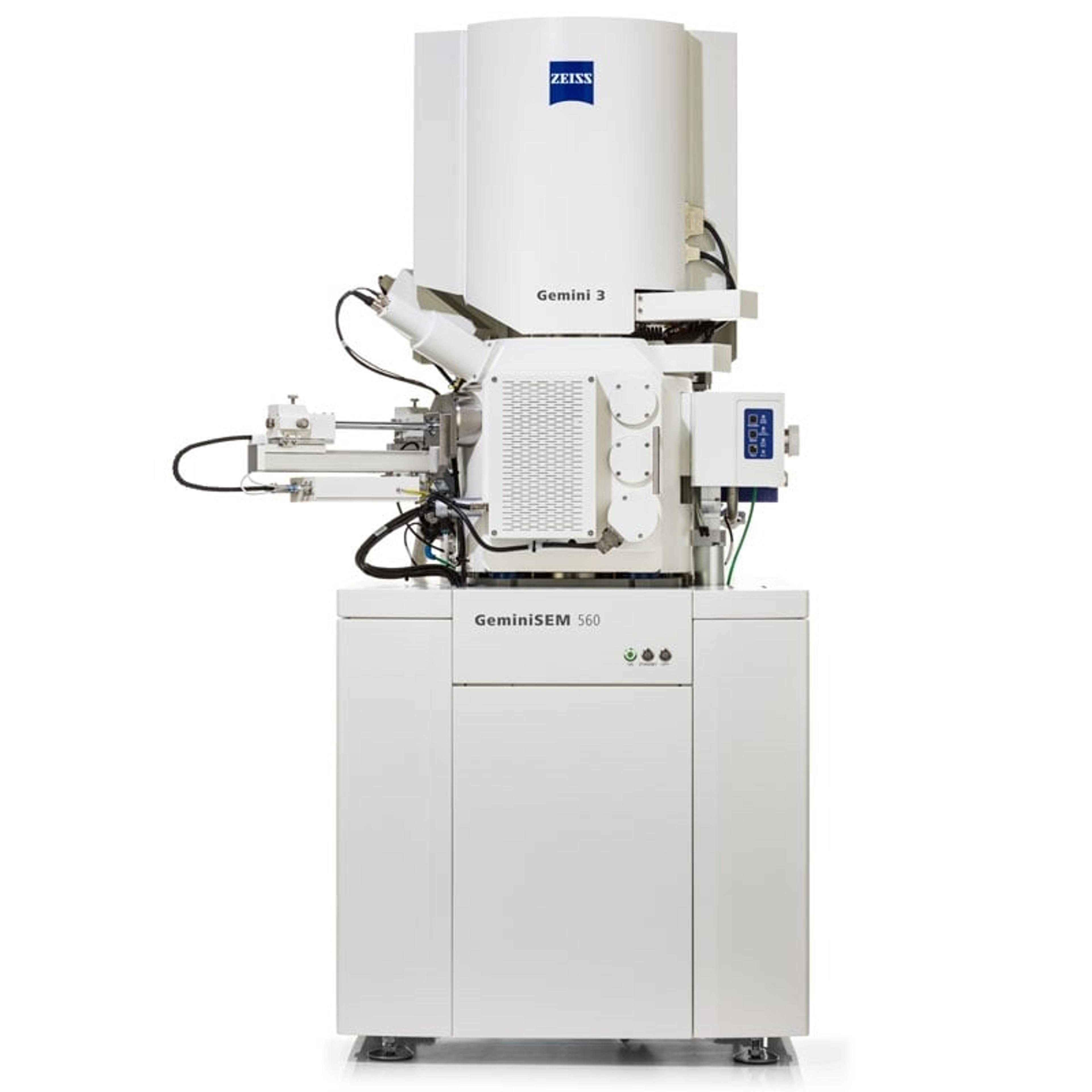
ZEISS GeminiSEM Family
ZEISS Research Microscopy SolutionsFor Your Highest Demands in Sub-nanometer Imaging, Analytics and Sample Flexibility