ZEISS Crossbeam 550 Sets New Standards in 3D Analytics and Sample Preparation
Enhanced resolution and faster FIB material processing for maximum efficiency
11 Sept 2017Product news
ZEISS presents a new generation of focused ion beam scanning electron microscopes (FIB-SEMs) for high-end applications in research and industry. ZEISS Crossbeam 550 features a significant increase in resolution for imaging and material characterization and a speed gain in sample preparation.
Nanostructures such as composites, metals, biomaterials or semiconductors can be investigated with analytical and imaging methods in parallel. ZEISS Crossbeam 550 allows simultaneous modification and monitoring of samples, resulting in fast sample preparation and high throughput e.g. for cross-sectioning, TEM lamella preparation or nano-patterning.
See the latest news in Materials here >>
ZEISS Crossbeam 550 provides best image quality in 2D and 3D. The new Tandem decel mode enables enhanced resolution together with a maximization of image contrast at low landing energies. The pioneering Gemini II electron optics delivers optimum resolution at low voltage and high probe current simultaneously. The FIB column combines the highest available FIB current of 100 nA with the new FastMill mode, allowing for highly precise and more efficient material processing and imaging in parallel. Additionally, the new process for automated emission recovery increases the user-friendliness and optimizes the FIB column for reproducible results during long-term experiments.
Material scientists profit from excellent 3D analytical properties, especially thanks to the also new, fully integrated module for 3D EDS analyses with ZEISS Atlas 5. In the life sciences, ZEISS Crossbeam 550 convinces with its enhanced resolution at low voltages and an outstanding stability for long-term 3D tomography. Moreover, it is possible to optimally integrate the new workstation into correlative workflows and to combine it with light, X-ray or ion beam microscopy.
ZEISS Crossbeam 550 replaces its predecessor ZEISS Crossbeam 540 and is available in a variation with a large chamber for the first time. Selected product features can be upgraded for existing ZEISS Crossbeam 540 owners.
A webinar on May 4, 2017 provides information on the advantages of ZEISS Crossbeam 550.
Have you used ZEISS products? Leave a review here
Related products
Request Quote for All Products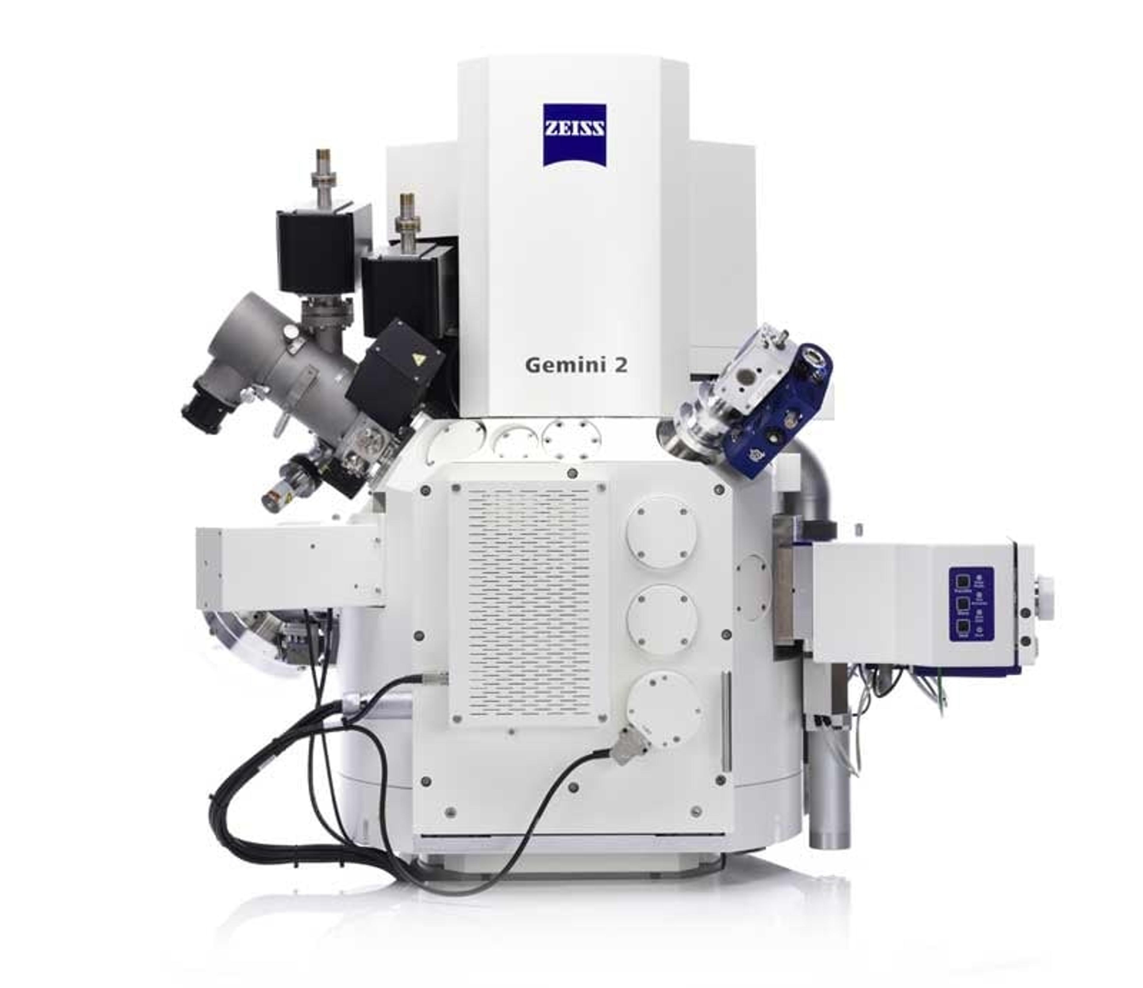
ZEISS Crossbeam Family
ZEISS Research Microscopy SolutionsWithin ZEISS Crossbeam Family you have the choice between Crossbeam 340 or Crossbeam 550. Exploit the variable pressure capabilities of Crossbeam 340. Or use Crossbeam 550 for your most demanding characterizations and choose the chamber size, standard or large, that best suits your samples.

ZEISS Atlas 5
ZEISS Research Microscopy SolutionsLarge area imaging for SEM, FE-SEM & FIB-SEM ATLAS combines a 16 bit scan generator and dual super-sampling signal acquisition hardware with image processing and control software for your ZEISS electron microscope. Acquire images up to 32 k x 32 k pixels, with dwell times from 100 ns to > 100 s, adjustable in 100 ns increments. Save your images with eight or sixteen bits of intensity. With the ATLAS “Mosaic Tool” you create large image montages, automatically moving from image tile to tile, and mosaic site to site, resulting in an “Extreme Field of View” image, at SEM nanometer scale resolution. ATLAS provides • reduced number of tiles to acquire, reducing stage motion delay and areal fraction of each image “lost” to overlap • reduced number of overlap “seams”, leading to less beam damage and degradation of the sample • reduced computational complexity