Thermo Scientific Talos F200E (S)TEM combines atomic-level imaging with fast EDS analysis
18 Mar 2021
Product news
Thermo Fisher Scientific has announced the launch of the Talos F200E Scanning Transmission Electron Microscope ((S)TEM), combining atomic-level resolution imaging, fast energy-dispersive X-ray spectroscopy (EDS) analysis, and enhanced data reliability, designed specifically for the semiconductor industry's increasing demand.
Advances in communications technologies supported by the transition to 5G are continuing to spur the need for semiconductor devices that offer greater energy efficiency and performance. Autonomous vehicles, AI, Industry 4.0, smart cities and the Internet of Things (IoT) are all driving development of smaller, more complex semiconductor structures. To deliver the high-volume, reproducible (S)TEM results necessary to support such demands at the atomic scale, the semiconductor industry needs efficient solutions for its research and development labs.
The Talos F200E (S)TEM offers automated alignment with its "Align Genie" feature as well as image distortion of ≤1%, enabling users to obtain quick, reliable and repeatable results. The optional DualX provides a larger EDS detector than previously available on the Talos F200X, enabling 1.5 times faster EDS analyses. The Talos F200E is a cost-effective and easy-to-use system, designed to allow semiconductor labs to achieve fast sample characterization, accelerate time to production, and improve manufacturing yields.
"As the pace of innovation continues to accelerate, semiconductor companies are requiring their analysis labs to speed turnaround times and deliver more reliable and repeatable (S)TEM data on a wide variety of devices and process technologies that support their businesses," said Glyn Davies, vice president of semiconductor at Thermo Fisher. "The Talos F200E enables customers to address these needs by delivering quality image data, fast chemical analysis and industry-leading defect characterization—in an affordable, easy-to-use instrument."
Want the latest science news straight to your inbox? Become a SelectScience member for free today>>
Related products
Request Quote for All Products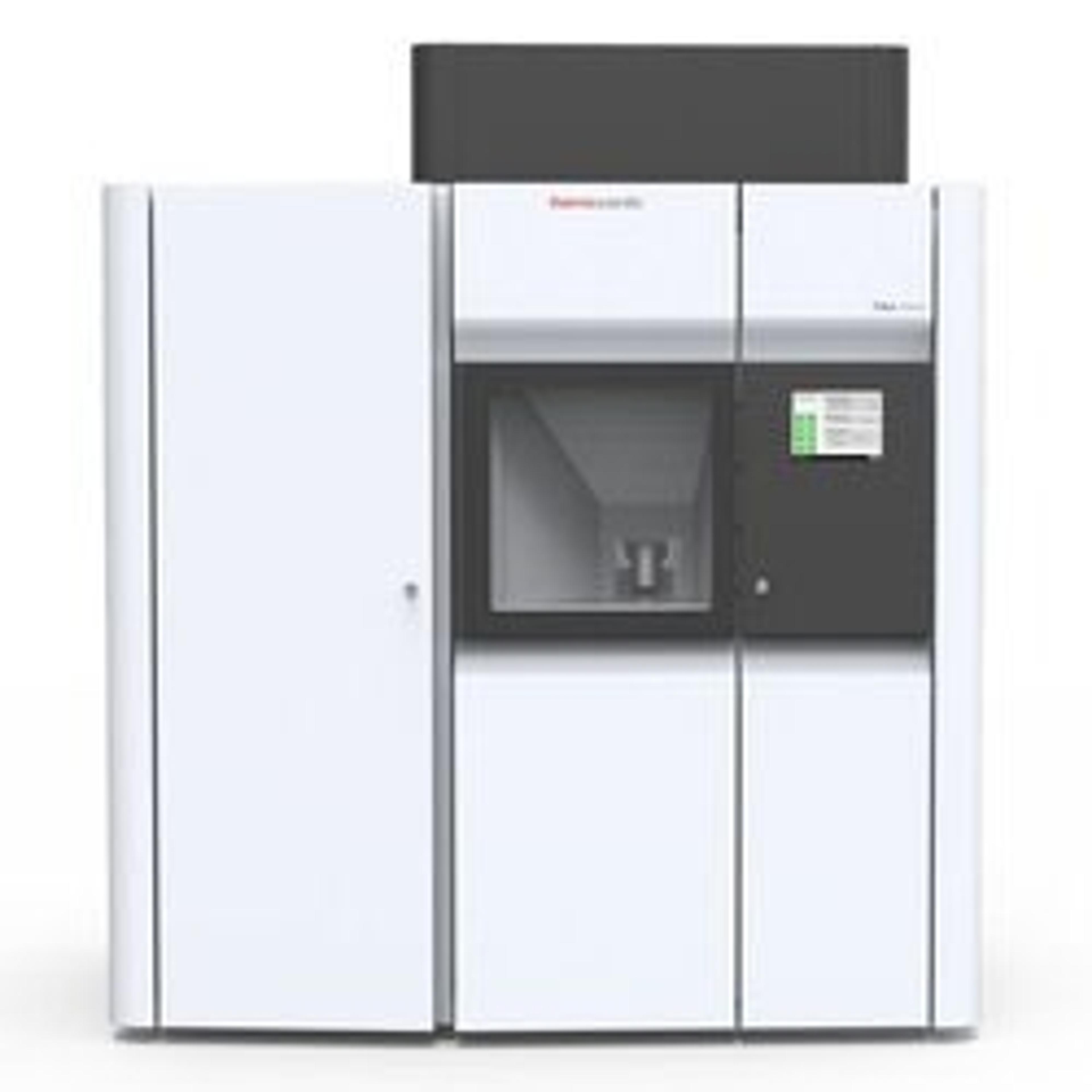
Thermo Scientific™ Talos™ Arctica™ TEM for Life Sciences
Thermo Fisher ScientificThe Thermo Scientific™ Talos™ Arctica™ is a 200kV FEG transmission and scanning electron microscope (S/TEM). It is a powerful, stable, and versatile system for delivering high-resolution 3D characterization of biological and biomaterials samples in cell biology, structural biology, and nanotechnology research.