New Ion Milling system for SEM Sample Prep
1 Sept 2011Product news
Hitachi High-Technologies has launched the IM4000 Ion Milling system. Used to prepare specimens for scanning electron microscope (SEM) imaging and analytical studies such as EDX and EBSP, the versatile IM4000 is capable of both pin-point cross-section and flat surface ion milling. Cross-section milling provides smooth cross-section specimens for high resolution imaging of subsurface structures, with the cross section position accurately controllable by fine positioning of a beam-shielding mask edge. Flat milling provides uniform polishing of surfaces of 5 mm diameter or more with variable angle milling, to either flatten surfaces or to selectively enhance specimen surface features (relief milling).
The two IM4000 applications, cross section and flat surface milling, are realised via 2 different removable sample stage units, allowing for convenient specimen setting and cutting edge definition using an external optical microscope.
The IM4000 ion milling system features a new high-current Argon ion gun that delivers cross sectional milling rates of 300$)A&Lm/hr in Silicon for dramatically reduced cross-sectioning times. The wide Argon ion beam can define sharp cross sections even on samples of dissimilar materials with different hardness that cannot be cut or broken without causing material deformations or dislocations. Sensitive materials like polymers or papers can be processed by freely selecting proper lower ion beam energies between 0 and 6kV, without need for special sample cooling.
Wide and smooth flat milled surfaces of approximately 5mm in diameter or more can be achieved within minutes by shifting the centre of the defocused ion beam from the sample rotation or swinging centre. The beam irradiation angle to the specimen surface is selectable from 0$)A!c to 90!c. This makes the IM4000 useful in a multitude of different fields and applications such as materials, semiconductors, research and quality control.
Related products
Request Quote for All Products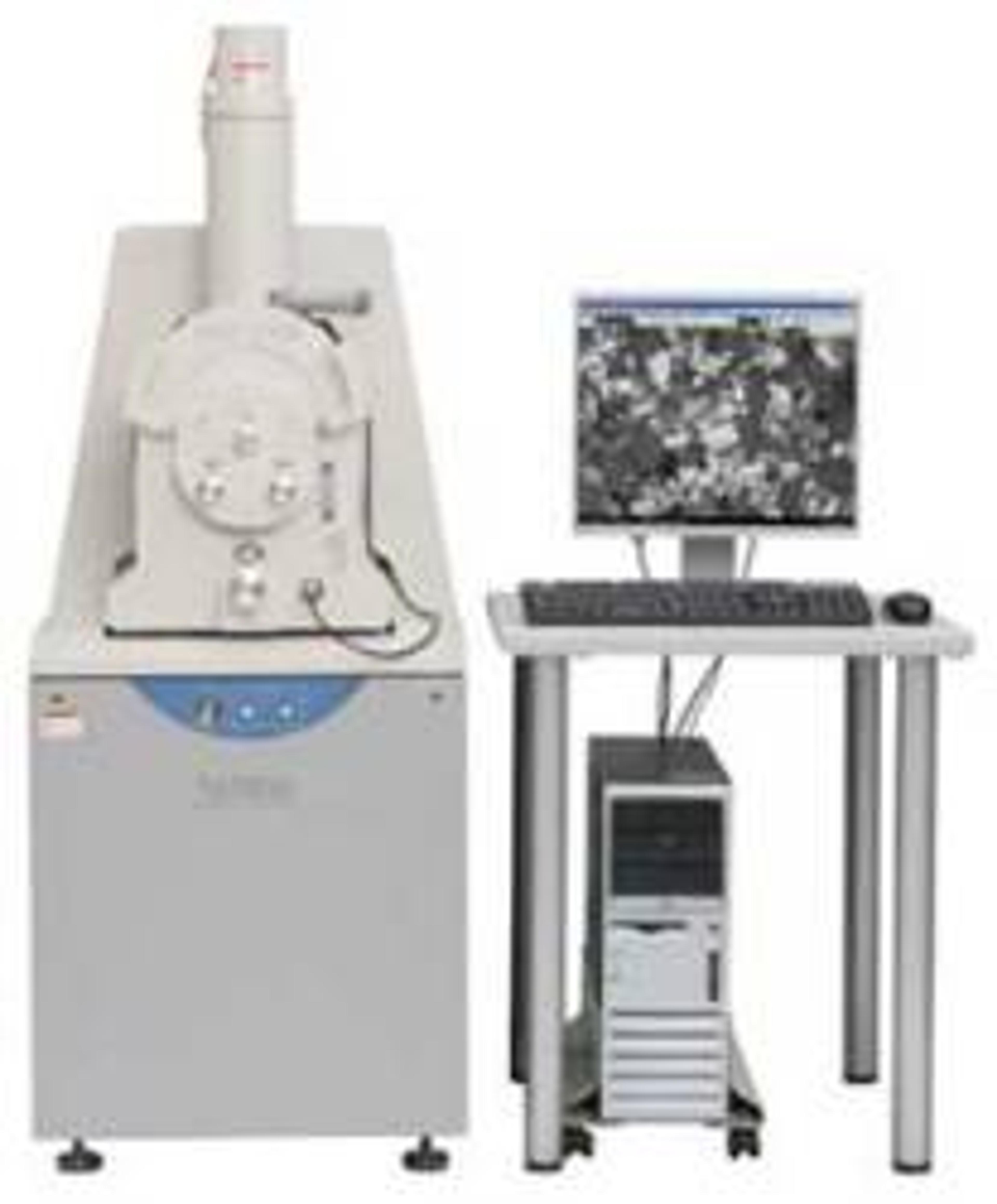
Hitachi VP-SEM SU1510
Hitachi High Technologies America, Inc.Hitachi VP-SEM SU1510 - Top performance in very compact size The new Hitachi SU1510 VP-SEM combines the high-performance electron optics of the S-3400N and S-3700N with an ultra-compact design. Its main body is only 55cm wide, and unlike conventional SEM design concepts the SU1510 does not require a special display and operating console - instead, monitor and PC controls can be conveniently placed on any user prepared workspace. All this does not restrict the available sample size - with up to 153mm sample diameter and 60mm sample height at EDX working distance the SU1510 does not fall short against its full-scale siblings.Features of the Hitachi VP-SEM SU1510 include:• VP-SEM mode available as standard (• Beam energy range 300eV to 30keV • 3nm SE resolution in high-vacuum mode (15 kV) • 4nm BSE resolution in VP-SEM mode • Everhardt-Thornley-SE detector, and 4-segment-BSE detector as standard. ESED detector and IR Chamberscope optionally available. • Quad-Bias function for superior signal-to-noise ratio at lower beam energies • TMP vacuum system with single rotary pump, no cooling water required. • Sophisticated automatic beam axis-alignment functions (Auto Beam Setting, Auto Axial Alignment, auto-Brightness, Auto-Stigma, Auto-Focus) • Animated operation and maintenance guides • Double EDX ports (opposing each other) with 35° take-off-angle, allowing EDX analysis on up to 60mm tall samples