Hysitron TI 980 TriboIndenter
24 Jul 2023In this application note, Bruker Nano provides a detailed overview of the Hysitron® TI 980 TriboIndenter®. This nanomechanical test instrument builds upon decades of Hysitron technological innovation to deliver new levels of performance, enhanced capabilities, and improved versatility in nanomechanical characterization. The Hysitron TI 980 has been designed to achieve remarkable advances in control and throughput capabilities, testing flexibility, applicability, measurement reliability, and system modularity.
Related products
Request Quote for All Products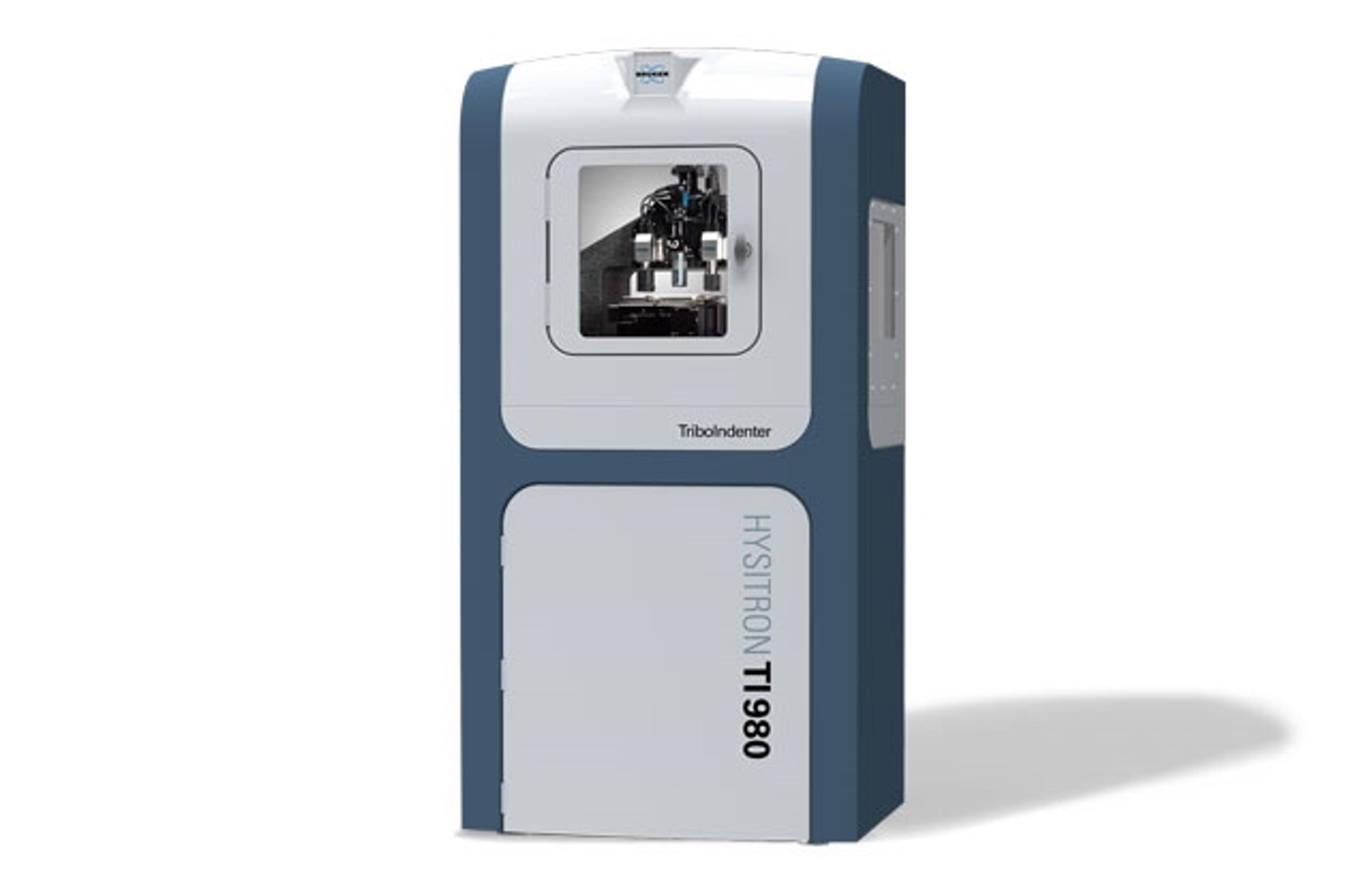
Hysitron TI 980
Bruker Nano Surfaces and MetrologyThe Hysitron TI 980 nanoindenter achieves remarkable advances in control and throughput capabilities, testing flexibility, applicability, measurement reliability, and system modularity. This industry-leading system builds upon decades of Hysitron technological innovation to deliver new levels of extraordinary performance, enhanced capabilities, and ultimate versatility in nanomechanical characterization.