How Ultra-Advanced FIB-SEM Microscopes are Accelerating Materials Discovery & Design
Learn everything you need to know about ZEISS Crossbeam with these exclusive expert interviews and free article downloads
6 Mar 2018
Editorial article
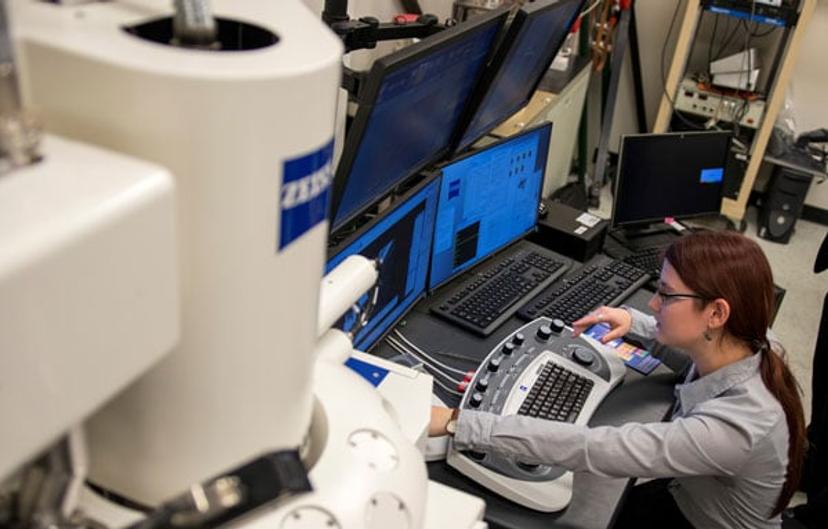
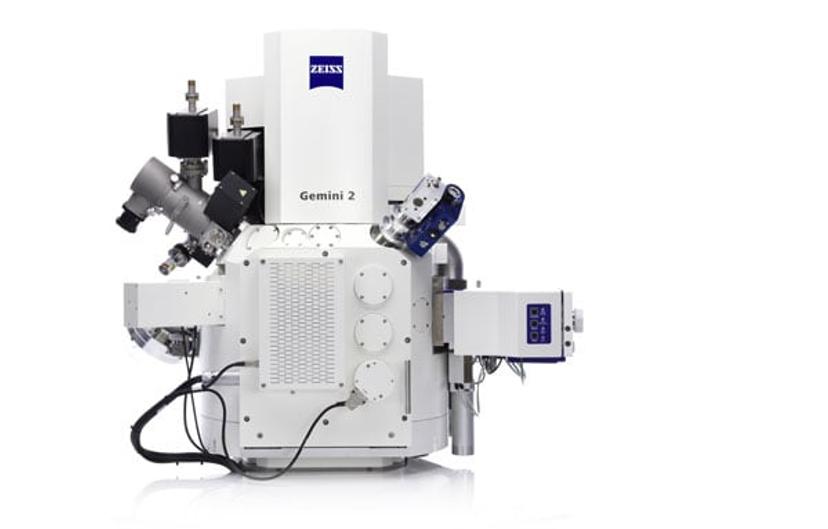
The ZEISS Crossbeam family of FIB-SEM microscopes combine the imaging and analytical performance of a field emission scanning electron microscope (FE-SEM) with the processing ability of a focused ion beam (FIB).
With ZEISS Crossbeam you combine the electron optics of the Gemini column with the ability of a next-generation FIB for material processing and sample preparation on a nanoscopic scale. You can use the modular platform concept and the open and easily extendable software architecture of this 3D nano-workstation for high-throughput nanotomography and nanofabrication of even the most demanding, charging or magnetic samples.
Thought-leaders around the world are using ZEISS Crossbeam in their groundbreaking research. Read these exclusive interviews to learn more:
Could Correlative Microscopy Solve the Energy Problems of the Future?
The Materials Research Institute (IMFAA), at Aalen University of Applied Sciences, Germany, focuses on the application and further development of materialography methods. SelectScience® speaks to Dr. Timo Bernthaler, materials scientist at IMFAA, to find out how microscopy is helping to advance this important research.
Use of Correlative Imaging to Bridge the Materials Gap Between Scientific Disciplines
Dr. Richard Johnston is an associate professor in the Material Research Centre, Swansea University, Wales, UK. Johnston leads a research group focused on imaging, with a particular emphasis on X-ray microscopy, and is the co-director of the Advanced Imaging of Materials (AIM) center. As an expert in the field of correlative imaging, and an advocate of collaboration between diverse scientific fields, Johnston’s work is bridging the gap between disciplines. Read this exclusive SelectScience® interview to find out more.
Correlating Structural and Mechanical Properties Over Time: The Fourth Dimension of Materials Science
Nikhilesh Chawla is Fulton Professor of Materials Science and Engineering (MSE) at Arizona State University, Tempe, USA, where he studies the mechanical behavior and modeling of advanced materials. In this exclusive interview, SelectScience® speaks to Prof. Chawla to find out more about his work.
Free related application notes to download:
ZEISS Crossbeam - Enabling Smart FIB Work with SmartSEM
This application note describes SmartFIB, a new user interface for FIB operation in ZEISS Crossbeam instruments, and some of its capabilities. SmartFIB is an extension of SmartSEM, the operating software of ZEISS scanning electron microscopes, which is active for ZEISS FIB-SEM systems. When milling an object by focused ion beam (FIB), it is essential to control a large set of patterning parameters. These define the so-called FIB milling strategy. Minor changes in the milling strategy can have a dramatic impact on the results achieved. SmartFIB enables the user to flexibly tailor their FIB milling strategy to obtain the desired results, by providing access to all relevant parameters like dose, pixel spacing, pixel dwell time and FIB current.
Correlative Microscopy Protocols: A Reference Guide to Correlative Sample Preparation
This document provides an overview of existing sample preparation know-how for correlative microscopy. While many of the cited protocols still reference TEM they are typically applicable to the modern technique of field emission SEM with little or no modifications.
Local Charge Compensation in SEM Material Analysis
In this application note, high-resolution SEM imaging is executed on non-conductive samples by the integration of a charge compensation system.
Microstructure of Skin Cream Using Cryo-planing and Cryo-FIB-SEM
Soft materials containing water or other solvents, such as home and personal care products, are not high vacuum compatible. Therefore, it is difficult to expose their microstructure. This application article demonstrates the use of cryo-SEM and cryo-FIB-SEM techniques in exposing the microstructure of a soft material, using face cream as an example.
Characterization of Solid Oxide Electrolysis Cells by Advanced Focused Ion Beam-SEM Tomography
This white paper investigates the microstructural changes after cycling of a solid oxide electrolysis cell (SOEC), studied by means of focused ion beam (FIB)-SEM tomography. The advanced tomography package, ZEISS Atlas 5 3D Tomography, enables high-resolution 3D electron imaging and 3D energy dispersive X-ray spectroscopy (EDS) elemental imaging, using two different sets of SEM conditions optimized for the respective task.
Multi-Scale Correlative Study of Corrosion Evolution in a Magnesium Alloy
This application note describes the results of a multi-scale correlative tomography study on the corrosion of a magnesium alloy ZEISS Atlas 5 is used to efficiently link and navigate between different microscopic modalities, e.g. in situ sub-micron X-ray microscopy, nanoscale X-ray microscopy and FIB-SEM tomography. The study provides a description of the complex crack and corrosion byproduct geometries which can lead to a more complete understanding of the underlying mechanisms for corrosion.
Visit the SelectScience product directory to learn more about the ZEISS Crossbeam product family
Related products
Request Quote for All Products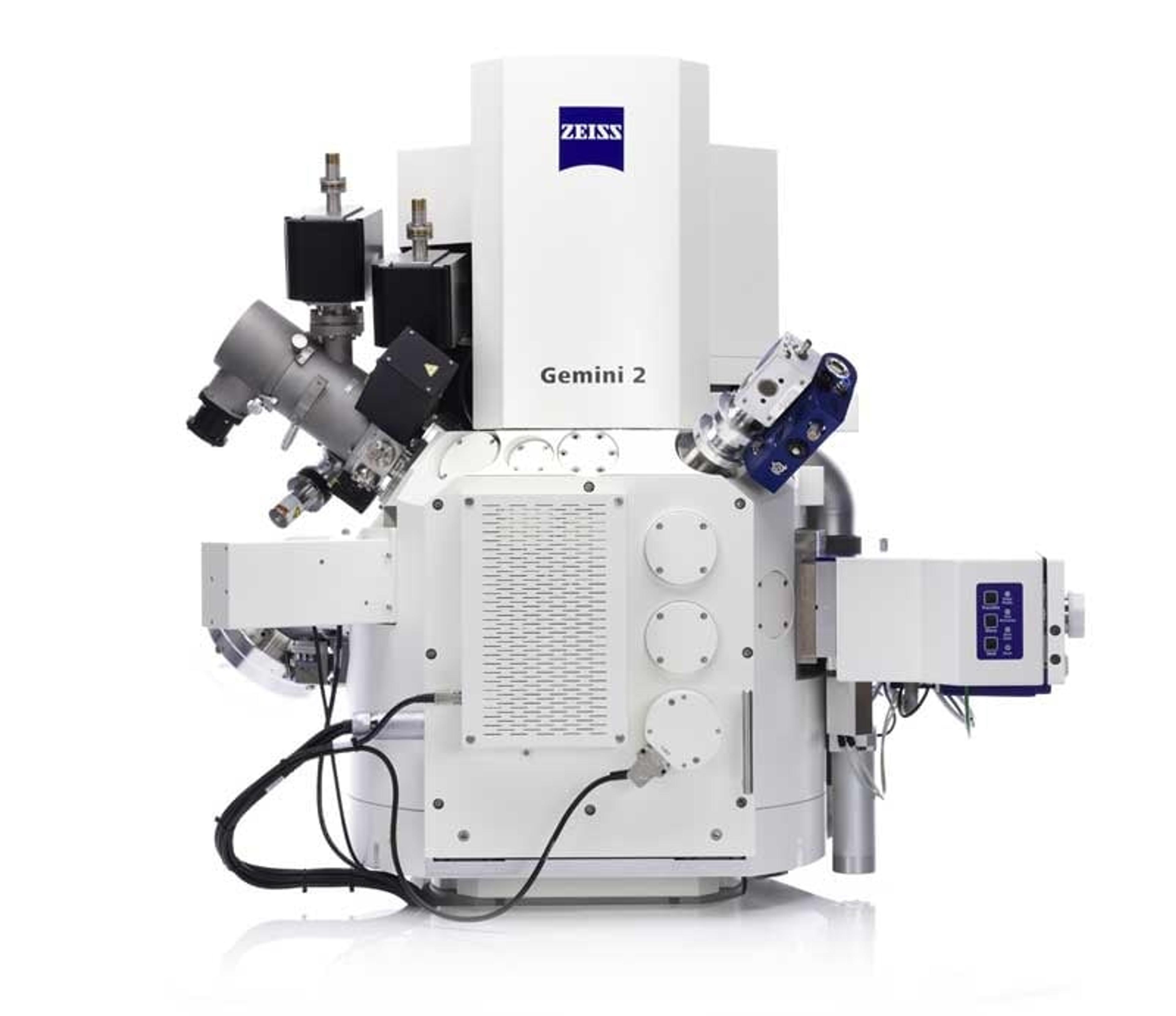
ZEISS Crossbeam Family
ZEISS Research Microscopy SolutionsWithin ZEISS Crossbeam Family you have the choice between Crossbeam 340 or Crossbeam 550. Exploit the variable pressure capabilities of Crossbeam 340. Or use Crossbeam 550 for your most demanding characterizations and choose the chamber size, standard or large, that best suits your samples.