Array Tomography with ZEISS Scanning Electron Microscopes
Reduce your time to result with automated nano-imaging of large samples: image your serial sections fast and efficiently
24 Apr 2016
Industry news
ZEISS Microscopy and RMC-Boeckeler recently organized customer workshops on the topic of array tomography. The workshops in Germany and Australia, hosted by the ZEISS Microscopy Labs in Munich and the Centre for Advanced Microscopy in Canberra highlighted the growing interest into high throughput 3D electron microscopy approaches for life sciences. With array tomography solutions such as ATUMtome with Atlas 5 and ZEISS FE-SEM instruments or the unique ZEISS MultiSEM 505, the world’s fastest scanning electron microscope, ZEISS enables industry and research with the fastest automated imaging throughput at highest resolutions.
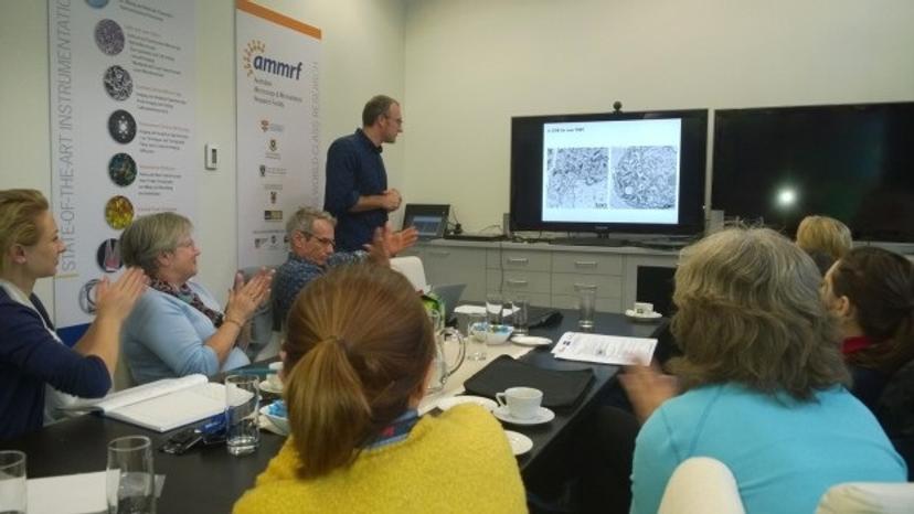
ZEISS & RMC-Boeckeler Array Tomography Workshop in Canberra
Scanning electron microscopy is capable of imaging biological microstructures at amazing resolution and can be combined with 3D imaging to provide further insight. Various techniques can be employed to image samples in 3D, many of which have only recently become accessible to the research community. The fully booked workshops provided an overview of recent strides in instrumentation development. These advances have the potential to do for electron microscopy what confocal microscopy did for light microscopy.

ZEISS & RMC-Boeckeler Workshop in the ZEISS Microscopy Labs, Munich
In his presentation Trevor Hinwood (Distributor for RMC) explored sample preparation techniques for the use of scanning electron microscopy in back scatter electron detection mode which produces images quite equivalent to TEM images at magnifications up to 10,000x. Steve Pfeiffer (RMC-Boeckeler) presented 3D methods including serial block face SEM (3View, SBFSEM), focused ion beam (FIB-SEM) and the automatic tape-collecting microtome (ATUMtome). All of these techniques have the capability of producing thousands of images or sections in serial order. Terence Da Silva (ZEISS Microscopy) introduced ZEISS Atlas 5 Array Tomography with an automated approach to image acquisition and data collection. The workshop participants Eric Hannsen (University of Melbourne) and Rick Webb (University of Queensland) presented work done with their current imaging systems, also highlighting the future potential of these technologies.
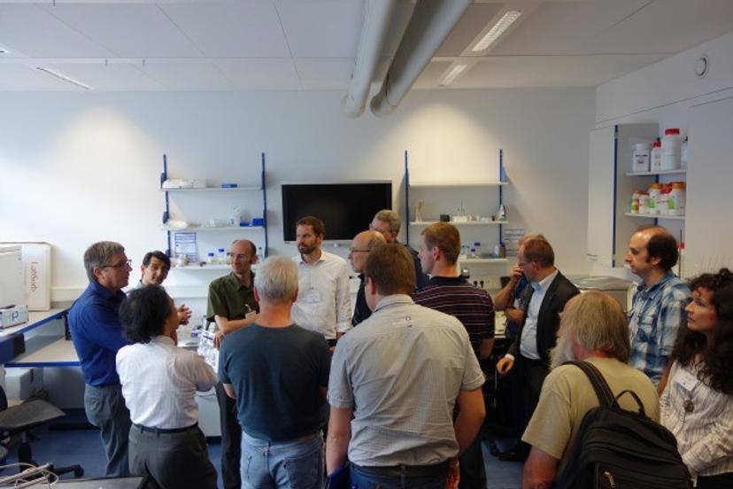
Richard Schalek (Harvard), co-inventor of the ATUMtome, at the ZEISS Microscopy Labs Munich
“It was a great opportunity to exchange ideas and experiences on sample preparation and 3D imaging of biological samples in SEM”, said Melanie Rug, manager of the Center for Advanced Microscopy (CAM) and host of the event. Similar joint workshops between ZEISS and RMC-Boeckler were held at the ZEISS Microscopy Labs in Munich with key speakers such as Richard Schalek (Harvard) and Christel Genoud (FMI, Basel).
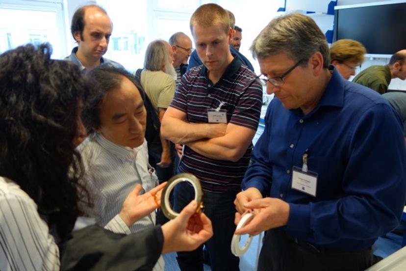
Taking a closer look at the tape collecting workflow for array tomography
“The workshop in Canberra was a direct transfer of the successful concept to our local customer community and a great collaboration between CAM, RMC-Boeckler and ZEISS” said Rene Hessling, Head of the Microscopy Division for ZEISS Australasia.
Related products
Request Quote for All Products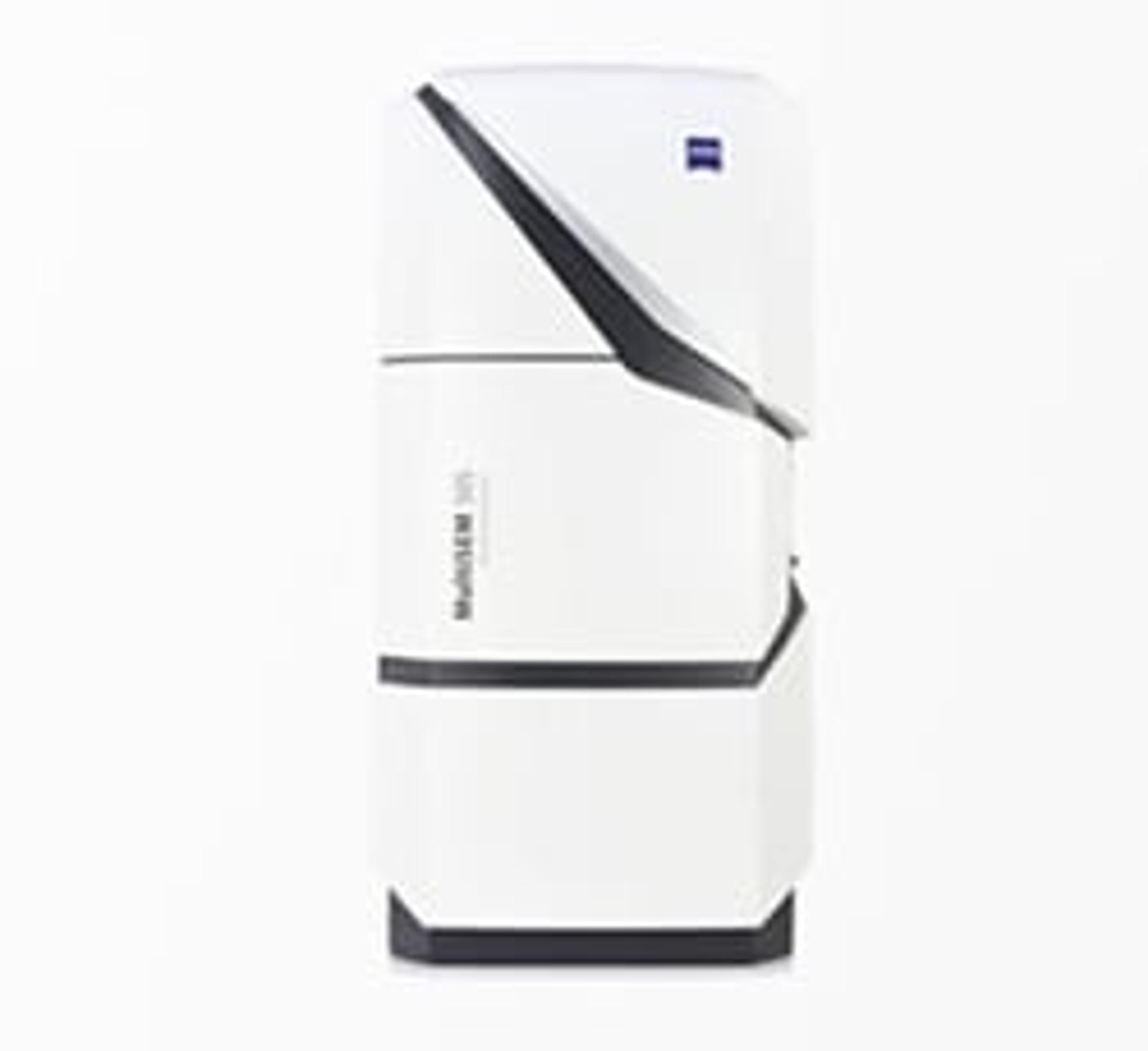
ZEISS MultiSEM Research Partner Program
ZEISS Research Microscopy SolutionsThe World's Fastest Scanning Electron Microscopes.