ResourceMaterials

Advancing materials engineering with microscopy

19 Jul 2024
microscopy eBook pages

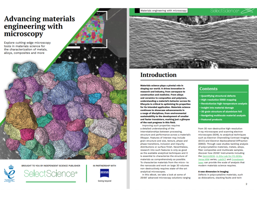
Materials science is crucial in shaping our world and driving innovation across various fields like aerospace, construction, and medicine. It involves understanding the behavior of materials such as alloys, ceramics, composites, and polymers throughout their lifecycle. This knowledge is essential for optimizing their properties for specific applications.

Download this expert guide for free today and explore advanced microscopy solutions from ZEISS, including 3D non-destructive high-resolution X-ray microscopes and scanning electron microscopes (SEM). The eBook also covers analytical techniques such as Electron Channelling Contrast Imaging (ECCI) and Electron Backscattered Diffraction (EBSD).

Plus, find case studies on polycrystalline materials, metals, alloys, fiber composites, and multiscale samples, and learn about the tools essential for modern materials science analysis.

Links

Tags

Electron MicroscopyElectron microscopes (EM) are used to create high-resolution images of samples at the nanoscale by means of an accelerated beam of electrons as a source of illumination. Types of electron microscope include scanning electron microscopes (SEM), transmission electron microscopes (TEM), scanning transmission electron microscopes (STEM) and cryo-electron microscopes. Focused ion beam (FIB) microscopes are useful for modifying or milling a sample surface with nanometer precision, as well as imaging. Find the best electron microscopes in our peer-reviewed product directory: compare products, check customer reviews and receive pricing direct from manufacturers.Light MicroscopyLight microscopes or optical microscopes are used to visualize microscale objects under magnification, including cells, clinical specimens and materials. Lab equipment for light microscopy includes confocal microscopes, fluorescence microscopes, zoom and stereo microscopes. Microscope slides and imaging reagents are available for visualizing samples, as well as various microscope stages and incubators for large or temperature-sensitive samples. Find the best light microscopes in our peer-reviewed product directory: compare products, check customer reviews and receive pricing direct from manufacturers.Atomic Force Microscopy / Scanning Tunneling MicroscopyAtomic force microscopes (AFM) and scanning tunneling microscopes (STM) are high-resolution forms of scanning probe microscope (SPM) used to generate topological information of a sample down to the atomic scale. Instruments can generate an image of the surface topology, manipulate objects and reveal information on localized properties such as Young’s modulus, conductivity, and magnetism. High-quality STM and AFM probes optimized for your application are available, as well as other SPM-based instruments such as scanning ion conductance microscopes (SICM) & near-field scanning optical microscopes (NSOM). Find the best AFM and STM equipment in our peer-reviewed product directory: compare products, check customer reviews and receive pricing direct from manufacturers.X-Ray Diffraction and SpectroscopyX-Ray diffraction & spectroscopy are used in material characterization to discern the structure and elemental composition of a sample. X-Ray diffractometers (XRD) are superior instruments in elucidating the dimensional atomic structure of crystalline materials, including powders, thin films and single crystals. For large unit cells or ordered macromolecules, consider small-angle X-ray scattering (SAXS). X-ray spectroscopic techniques include X-ray fluorescence (XRF) and X-ray photoelectron spectroscopy (XPS), both providing simple and accurate methods for determining the elemental composition of a material. Energy dispersive (EDXRF) and wavelength dispersive (WDXRF) XRF spectrometers are available, as well as handheld/portable devices. High-resolution, 3D microstructure characterization of materials can be achieved with X-ray microscopes combining sub-micron resolution imaging with 3D computed tomography. Find the best XRD and XRF spectrometers in our peer-reviewed product directory: compare products, check customer reviews and receive pricing direct from manufacturers.X-ray CrystallographyX-ray crystallography is an analytical technique used to determine the arrangement of atoms in a crystal. Monochromatic x-rays are produced from a synchrotron or x-ray generator. An x-ray crystallography system uses a detector to measure the x-ray diffraction from the crystal. The information is used to generate a 3D image of the crystal.MicroscopyMicroscopy is a technique used to observe small objects in detail, from cells to materials, using light or electron microscopes. It enables researchers to examine structures with high resolution, aiding in fields such as biology, medicine, and materials science. With advanced microscopy techniques, scientists can gain insights into cellular processes, tissue structures, and material properties. Explore the best microscopy solutions in our peer-reviewed product directory, compare products, read customer reviews, and get pricing directly from manufacturers.SEMScanning Electron Microscopy (SEM) is a technique that uses a focused electron beam to scan a sample and create high-resolution images. It is widely used in materials science, nanotechnology, and biological research. Explore SEM systems in our peer-reviewed product directory; compare products, check reviews, and get pricing directly from manufacturers.FIB-SEMMaterial CharacterizationMaterialsX-ray MicroscopyGrain Boundariesdefect analysis